

Литература 1-й семетр / Литература 1-й семетр / Память / Microware(3-х проводной интерфейс) / AT93C46
.PDFFeatures
•Low-Voltage and Standard-Voltage Operation
–5.0 (V CC = 4.5V to 5.5V)
–2.7 (V CC = 2.7V to 5.5V)
–2.5 (V CC = 2.5V to 5.5V)
•3-Wire Serial Interface
•Schmitt Trigger, Filtered Inputs for Noise Suppression
•2 MHz Clock Rate (5V) Compatibility
•Self-Timed Write Cycle (10 ms max)
•High Reliability
–Endurance: 1 Million Write Cycles
–Data Retention: 100 Years
–ESD Protection: >4000V
•Automotive Grade and Extended Temperature Devices Available
•8-Pin PDIP and JEDEC SOIC Packages
Description
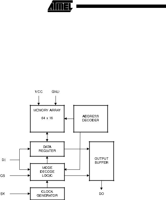
The AT93C46C provides 1024 bits of serial electrically-erasable programmable read only memory (EEPROM) organized as 64 words of 16 bits each. The device is optimized for use in many industrial and commercial applications where low-power and low-voltage operation are essential. The AT93C46C is available in space saving 8-pin PDIP and 8-pin JEDEC SOIC packages.
The AT93C46C is enabled through the Chip Select pin (CS), and accessed via a 3- wire serial interface consisting of Data Input (DI), Data Output (DO), and Shift Clock (SK). Upon receiving a READ instruction at DI, the address is decoded and the data is clocked out serially on the data output pin DO. The WRITE cycle is completely selftimed and no separate ERASE cycle is required before WRITE. The WRITE cycle is only enabled when the part is in the ERASE/WRITE ENABLE state. When CS is brought “high” following the initiation of a WRITE cycle, the DO pin outputs the READY/BUSY status of the part.
The AT93C46C is available in 4.5V to 5.5V, 2.7V to 5.5V, and 2.5V to 5.5V versions.
Pin Configurations
Pin Name |
Function |
|
|
|
|
CS |
Chip Select |
|
|
|
|
SK |
Serial Data Clock |
|
|
|
|
DI |
Serial Data Input |
|
|
|
|
DO |
Serial Data Output |
|
|
|
|
GND |
Ground |
|
|
|
|
VCC |
Power Supply |
|
|
|
|
NC |
No Connect |
|
|
|
|
DC |
Don’t Connect |
|
|
|
|
|
|
|
|
|
|
8-Pin PDIP
CS |
|
1 |
8 |
|
VCC |
|
|
||||
SK |
|
2 |
7 |
|
DC |
|
|
||||
DI |
|
3 |
6 |
|
NC |
|
|
||||
DO |
|
4 |
5 |
|
GND |
|
|
||||
|
|
|
|
|
|
8-Pin SOIC
CS |
|
1 |
|
8 |
|
VCC |
|
|
|
|
|||||
SK |
|
2 |
|
7 |
|
DC |
|
|
|
||||||
DI |
|
3 |
|
6 |
|
NC |
|
|
|
||||||
DO |
|
4 |
|
5 |
|
GND |
|
|
|
||||||
|
|
|
|
|
|
|
|
|
|
|
|
|
|
|
|
|
|
|
|
|
|
|
|
|
|
|
|
|
|
|
|
|
|
|
|
|
|
|
|
|
|
|
|
|
|
|
|
3-Wire |
Serial EEPROM |
1K (64 x 16) |
AT93C46C |
Rev. 1122A–07/98 |
1 |
Absolute Maximum Ratings*
Operating Temperature |
° |
° |
*NOTICE: Stresses beyond those listed under “Absolute |
-55 C to +125 C |
Maximum Ratings” may cause permanent dam- |
||
|
|
|
|
Storage Temperature ..................................... |
-65°C to +150°C |
age to the device. This is a stress rating only and |
|
|
|
|
functional operation of the device at these or any |
Voltage on Any Pin |
|
|
other conditions beyond those indicated in the |
with Respect to Ground ..................................... |
-1.0V to +7.0V |
operational sections of this specification is not |
|
Maximum Operating Voltage |
|
6.25V |
implied. Exposure to absolute maximum rating |
|
conditions for extended periods may affect |
||
DC Output Current |
|
5.0 mA |
device reliability. |
|
|
||
|
|
|
|
Block Diagram
2 |
AT93C46C |
|
|
||
|

AT93C46C
Pin Capacitance(1)
Applicable over recommended operating range from TA = 25°C, f = 1.0 MHz, V CC = +5.0V (unless otherwise noted).
Symbol |
|
Test Conditions |
Max |
Units |
Conditions |
|
|
|
|
|
|
COUT |
|
Output Capacitance (DO) |
5 |
pF |
VOUT = 0V |
CIN |
|
Input Capacitance (CS, SK, DI) |
5 |
pF |
VIN = 0V |
Note: 1. |
This parameter is characterized and is not 100% tested. |
|
|
|
|
DC Characteristics
Applicable over recommended operating range from: TAI = -40°C to +85°C, V CC = +2.5V to +5.5V, TAC = 0°C to +70°C, V CC = +2.5V to +5.5V (unless otherwise noted).
Symbol |
|
Parameter |
Test Condition |
Min |
Typ |
|
Max |
Units |
||||
|
|
|
|
|
|
|
|
|
|
|
||
VCC1 |
|
Supply Voltage |
|
|
|
2.5 |
|
|
5.5 |
V |
||
VCC2 |
|
Supply Voltage |
|
|
|
2.7 |
|
|
5.5 |
V |
||
VCC3 |
|
Supply Voltage |
|
|
|
4.5 |
|
|
5.5 |
V |
||
ICC |
|
|
Supply Current |
VCC = 5.0V |
|
READ at 1.0 MHz |
|
0.5 |
|
2.0 |
mA |
|
|
|
|
|
|
|
|
|
|
|
|||
|
|
|
WRITE at 1.0 MHz |
|
0.5 |
|
2.0 |
mA |
||||
|
|
|
|
|
|
|
|
|||||
|
|
|
|
|
|
|
|
|
|
|
|
|
ISB1 |
|
|
Standby Current |
VCC = 2.5V |
|
CS = 0V |
|
14.0 |
|
20.0 |
μA |
|
ISB2 |
|
|
Standby Current |
VCC = 2.7V |
|
CS = 0V |
|
14.0 |
|
20.0 |
μA |
|
ISB3 |
|
|
Standby Current |
VCC = 5.0V |
|
CS = 0V |
|
35.0 |
|
50.0 |
μA |
|
IIL |
|
|
Input Leakage |
VIN = 0V to VCC |
|
0.1 |
|
1.0 |
μA |
|||
IOL |
|
|
Output Leakage |
VIN = 0V to VCC |
|
0.1 |
|
1.0 |
μA |
|||
V |
(1) |
|
Input Low Voltage |
|
|
|
-0.6 |
|
V |
CC |
x 0.3 |
|
IL1 |
|
|
2.5V ≤ VCC |
≤ 5.5V |
|
|
|
|
V |
|||
|
(1) |
|
Input High Voltage |
VCC x 0.7 |
|
VCC + 1 |
||||||
VIH1 |
|
|
|
|
|
|
||||||
V |
|
|
Output Low Voltage |
|
|
IOL = 2.1 mA |
|
|
|
0.4 |
V |
|
OL1 |
|
|
4.5V ≤ VCC |
≤ 5.5V |
|
|
|
|
|
|
|
|
VOH1 |
|
Output High Voltage |
IOH = -0.4 mA |
2.4 |
|
|
|
|
V |
|||
|
|
|
|
|
|
|
||||||
V |
|
|
Output Low Voltage |
|
|
IOL = 0.15 mA |
|
|
|
0.2 |
V |
|
OL2 |
|
|
2.5V ≤ VCC |
≤ 2.7V |
|
|
|
|
|
|
|
|
VOH2 |
|
Output High Voltage |
IOH = -100 μA |
VCC - 0.2 |
|
|
|
|
V |
|||
|
|
|
|
|
|
|
||||||
Note: 1. |
VIL min and VIH max are reference only and are not tested. |
|
|
|
|
|
|
|||||
AC Characteristics
Applicable over recommended operating range from TA = -40°C to + 85°C, V CC = +2.5V to + 5.5V, CL = 1 TTL Gate and 100 pF (unless otherwise noted).
Symbol |
Parameter |
Test Condition |
Min |
Typ |
Max |
Units |
|
|
|
|
|
|
|
|
|
fSK |
SK Clock Frequency |
4.5V ≤ VCC |
≤ 5.5V |
0 |
|
2 |
MHz |
|
|
2.7V ≤ VCC |
≤ 5.5V |
0 |
|
1 |
|
|
|
2.5V ≤ VCC |
≤ 5.5V |
0 |
|
0.5 |
|
tSKH |
SK High Time |
4.5V ≤ VCC |
≤ 5.5V |
250 |
|
|
ns |
|
|
2.7V ≤ VCC |
≤ 5.5V |
250 |
|
|
|
|
|
2.5V ≤ VCC |
≤ 5.5V |
500 |
|
|
|
tSKL |
SK Low Time |
4.5V ≤ VCC |
≤ 5.5V |
250 |
|
|
ns |
|
|
2.7V ≤ VCC |
≤ 5.5V |
250 |
|
|
|
|
|
2.5V ≤ VCC |
≤ 5.5V |
500 |
|
|
|
3

AC Characteristics (Continued)
Applicable over recommended operating range from TA = -40°C to + 85°C, V CC = +2.5V to + 5.5V, CL = 1 TTL Gate and 100 pF (unless otherwise noted).
Symbol |
Parameter |
Test Condition |
|
|
|
Min |
Typ |
Max |
Units |
|
|
|
|
|
|
|
|
|
|
|
|
|
|
4.5V ≤ VCC |
≤ 5.5V |
|
|
250 |
|
|
|
|
tCS |
Minimum CS Low Time |
2.7V ≤ VCC |
≤ 5.5V |
|
|
250 |
|
|
ns |
|
|
|
2.5V ≤ VCC |
≤ 5.5V |
|
|
500 |
|
|
|
|
|
|
|
|
4.5V |
≤ VCC |
≤ 5.5V |
50 |
|
|
|
tCSS |
CS Setup Time |
Relative to SK |
2.7V ≤ VCC |
≤ 5.5V |
50 |
|
|
ns |
||
|
|
|
|
2.5V |
≤ VCC |
≤ 5.5V |
100 |
|
|
|
|
|
|
|
4.5V |
≤ VCC |
≤ 5.5V |
100 |
|
|
|
tDIS |
DI Setup Time |
Relative to SK |
2.7V ≤ VCC |
≤ 5.5V |
100 |
|
|
ns |
||
|
|
|
|
2.5V |
≤ VCC |
≤ 5.5V |
200 |
|
|
|
tCSH |
CS Hold Time |
Relative to SK |
|
|
|
0 |
|
|
ns |
|
|
|
|
|
4.5V |
≤ VCC |
≤ 5.5V |
100 |
|
|
|
tDIH |
DI Hold Time |
Relative to SK |
2.7V ≤ VCC |
≤ 5.5V |
100 |
|
|
ns |
||
|
|
|
|
2.5V |
≤ VCC |
≤ 5.5V |
200 |
|
|
|
|
|
|
|
4.5V |
≤ VCC |
≤ 5.5V |
|
|
250 |
|
tPD1 |
Output Delay to ‘1’ |
AC Test |
|
2.7V ≤ VCC |
≤ 5.5V |
|
|
250 |
ns |
|
|
|
|
|
2.5V |
≤ VCC |
≤ 5.5V |
|
|
500 |
|
|
|
|
|
4.5V |
≤ VCC |
≤ 5.5V |
|
|
250 |
|
tPD0 |
Output Delay to ‘0’ |
AC Test |
|
2.7V ≤ VCC |
≤ 5.5V |
|
|
250 |
ns |
|
|
|
|
|
2.5V |
≤ VCC |
≤ 5.5V |
|
|
500 |
|
|
|
|
|
4.5V |
≤ VCC |
≤ 5.5V |
|
|
250 |
|
tSV |
CS to Status Valid |
AC Test |
|
2.7V ≤ VCC |
≤ 5.5V |
|
|
250 |
ns |
|
|
|
|
|
2.5V |
≤ VCC |
≤ 5.5V |
|
|
500 |
|
|
|
AC Test |
|
4.5V |
≤ VCC ≤ 5.5V |
|
|
100 |
|
|
tDF |
CS to DO in High Impedance |
|
2.7V |
≤ VCC |
≤ 5.5V |
|
|
100 |
ns |
|
CS = VIL |
|
|
|
|||||||
|
|
|
2.5V |
≤ VCC |
≤ 5.5V |
|
|
200 |
|
|
|
|
|
|
|
|
|
||||
tWP |
Write Cycle Time |
|
|
|
|
|
0.1 |
|
10 |
ms |
|
|
|
|
|
|
|
|
|
||
|
|
4.5V |
≤ VCC |
≤ 5.5V |
|
1 |
|
ms |
||
|
|
|
|
|
|
|||||
Endurance(1) |
5.0V, 25°C, Page Mode |
|
|
|
|
|
1 M |
|
|
Write Cycle |
Note: 1. This parameter is characterized and is not 100% tested.
4 |
AT93C46C |
|
|
||
|

AT93C46C
Instruction Set for the AT93C46C
|
|
|
Address |
|
Instruction |
SB |
Op Code |
|
Comments |
x 16 |
||||
|
|
|
|
|
READ |
1 |
10 |
A5 - A0 |
Reads data stored in memory, at specified address. |
|
|
|
|
|
EWEN |
1 |
00 |
11XXXX |
Write enable must precede all programming modes. |
|
|
|
|
|
ERASE |
1 |
11 |
A5 - A0 |
Erase memory location An - A0. |
|
|
|
|
|
WRITE |
1 |
01 |
A5 - A0 |
Writes memory location An - A0. |
|
|
|
|
|
ERAL |
1 |
00 |
10XXXX |
Erases all memory locations. Valid only at VCC = 4.5V to 5.5V. |
WRAL |
1 |
00 |
01XXXX |
Writes all memory locations. Valid only at VCC = 4.5V to 5.5V. |
|
|
|
|
|
EWDS |
1 |
00 |
00XXXX |
Disables all programming instructions. |
|
|
|
|
|
Functional Description
The AT93C46C is accessed via a simple and versatile three-wire serial communication interface. Device operation is controlled by seven instructions issued by the host processor. A valid instruction starts with a rising edge of CS and consists of a Start Bit (logic “1”) followed by the appropriate Op Code and the desired memory Address location.
READ (READ): The Read (READ) instruction contains the Address code for the memory location to be read. After the instruction and address are decoded, data from the selected memory location is available at the serial output pin DO. Output data changes are synchronized with the rising edges of serial clock SK. It should be noted that a dummy bit (logic “0”) precedes the 16-bit data output string.
ERASE/WRITE (EWEN): To assure data integrity, the part automatically goes into the Erase/Write Disable (EWDS) state when power is first applied. An Erase/Write Enable (EWEN) instruction must be executed first before any programming instructions can be carried out. Please note that once in the Erase/Write Enable state, programming remains enabled until an Erase/Write Disable (EWDS) instruction is executed or VCC power is removed from the part.
ERASE (ERASE): The Erase (ERASE) instruction programs all bits in the specified memory location to the logical “1” state. The self-timed erase cycle starts once the ERASE instruction and address are decoded. The DO pin outputs the READY/BUSY status of the part if CS is brought high after being kept low for a minimum of 250 ns (tCS). A logic “1” at pin DO indicates that the selected memory location has been erased, and the part is ready for another instruction.
WRITE (WRITE): The Write (WRITE) instruction contains the 16 bits of data to be written into the specified memory location. The self-timed programming cycle tWP starts after the last bit of data is received at serial data input pin DI. The DO pin outputs the READY/BUSY status of the part if CS is brought high after being kept low for a minimum of 250 ns (tCS). A logic “0” at DO indicates that programming is still in progress. A logic “1” indicates that the memory location at the specified address has been written with the data pattern contained in the instruction and the part is ready for further instructions. A Ready/Busy Status cannot be obtained if the CS is brought high after the end of the self-timed programming cycle, tWP.
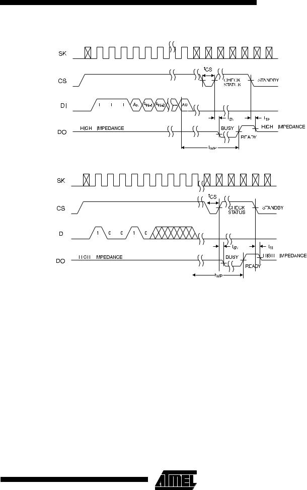
ERASE ALL (ERAL): The Erase All (ERAL) instruction programs every bit in the memory array to the logic “1” state and is primarily used for testing purposes. The DO pin outputs the READY/BUSY status of the part if CS is brought high after being kept low for a minimum of 250 ns (tCS). The ERAL instruction is valid only at VCC = 5.0V ± 10%.
WRITE ALL (WRAL): The Write All (WRAL) instruction programs all memory locations with the data patterns specifi ed in the ins tr uc tion . The DO pi n ou tputs th e READY/BUSY status of the part if CS is brought high after being kept low for a minimum of 250 ns (tCS). The WRAL instruction is valid only at VCC = 5.0V ± 10%.
ERASE/WRITE DISABLE (EWDS): To protect against accidental data disturb, the Erase/Write Disable (EWDS) instruction disables all programming modes and should be executed after all programming operations. The operation of the READ instruction is independent of both the EWEN and EWDS instructions and can be executed at any time.
5

Timing Diagrams
Synchronous Data Timing
Note: 1. This is the minimum SK period.
6 |
AT93C46C |
|
|
||
|

Organization Key for Timing Diagrams
|
AT93C46C |
|
|
I/O |
x 16 |
|
|
AN |
A5 |
|
|
DN |
D15 |
|
|
READ Timing |
|
|
|
CS |
|
|
|
SK |
|
|
|
DI |
1 1 0 AN |
... |
A0 |
|
|||
DO |
|
|
0 DN ... |
EWEN Timing(1)
Note: 1. Requires a minimum of nine clock cycles.
EWDS Timing(1)
Note: 1. Requires a minimum of nine clock cycles.
AT93C46C
tCS
D0
7
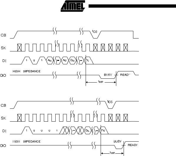
WRITE Timing
WRAL Timing(1)(2)
Notes: 1. Valid only at VCC = 4.5V to 5.5V.
2.Requires a minimum of nine clock cycles.
8 |
AT93C46C |
|
|
||
|
AT93C46C
ERASE Timing
TERAL Timing(1)
|
|
|
|
|
|
|
|
|
|
|
|
|
|
|
|
|
|
|
|
|
|
|
|
|
|
|
|
|
|
|
|
|
|
|
|
|
|
|
|
|
|
|
|
|
|
|
|
|
|
|
|
|
|
|
|
|
|
|
|
|
|
|
|
|
|
|
|
|
|
|
|
|
|
|
|
|
|
|
|
|
|
|
|
|
|
|
|
|
|
|
|
|
|
|
|
|
|
|
|
|
|
|
|
|
|
|
|
|
|
|
|
|
|
|
|
|
|
|
|
|
|
|
|
|
|
|
|
|
|
|
|
|
|
|
|
|
|
|
|
|
|
|
|
|
|
|
|
|
|
|
|
|
|
|
|
|
|
|
|
|
|
|
|
|
|
|
|
|
|
|
|
|
|
|
|
|
|
|
|
|
|
|
|
|
|
|
|
|
|
|
|
|
|
|
|
|
|
|
|
|
|
|
|
|
|
|
|
|
|
|
|
|
|
|
|
|
|
|
|
|
|
|
|
|
|
|
|
|
|
|
|
|
|
|
|
|
|
|
|
|
|
|
|
|
|
|
|
|
|
|
|
|
|
|
|
|
|
|
|
|
|
|
|
|
|
|
|
|
|
|
|
|
|
|
|
|
|
|
|
|
|
|
|
|
|
|
|
|
|
|
|
|
|
|
|
|
|
|
|
|
|
|
|
|
|
Note: |
1. Valid only at VCC = 4.5V to 5.5V. |
|
|
|
|
|
|
|
|
|
|
|||||
9

Ordering Information
tWP (max) |
ICC (max) |
ISB (max) |
fMAX |
|
|
|
(ms) |
(µA) |
(µA) |
(kHz) |
Ordering Code |
Package |
Operation Range |
|
|
|
|
|
|
|
10 |
2000 |
50.0 |
2000 |
AT93C46C-10PC |
8P3 |
Commercial |
|
|
|
|
AT93C46C-10SC |
8S1 |
(0°C to 70°C) |
|
|
|
|
|
|
|
10 |
2000 |
50.0 |
2000 |
AT93C46C-10PI |
8P3 |
Industrial |
|
|
|
|
AT93C46C-10SI |
8S1 |
(-40°C to 85°C) |
|
|
|
|
|
|
|
10 |
800 |
20.0 |
1000 |
AT93C46C-10PC-2.7 |
8P3 |
Commercial |
|
|
|
|
AT93C46C-10SC-2.7 |
8S1 |
(0°C to 70°C) |
|
|
|
|
|
|
|
10 |
800 |
20.0 |
1000 |
AT93C46C-10PI-2.7 |
8P3 |
Industrial |
|
|
|
|
AT93C46C-10SI-2.7 |
8S1 |
(-40°C to 85°C) |
|
|
|
|
|
|
|
10 |
600 |
20.0 |
500 |
AT93C46C-10PC-2.5 |
8P3 |
Commercial |
|
|
|
|
AT93C46C-10SC-2.5 |
8S1 |
(0°C to 70°C) |
|
|
|
|
|
|
|
10 |
600 |
20.0 |
500 |
AT93C46C-10PI-2.5 |
8P3 |
Industrial |
|
|
|
|
AT93C46C-10SI-2.5 |
8S1 |
(-40°C to 85°C) |
|
|
|
|
|
|
|
|
Package Type |
|
|
8P3 |
8-Lead, 0.300" Wide, Plastic Dual Inline Package (PDIP) |
|
|
8S1 |
8-Lead, 0.150" Wide, Plastic Gull Wing Small Outline (JEDEC SOIC) |
|
|
|
Options |
|
|
Blank |
Standard Device (4.5V to 5.5V) |
|
|
-2.7 |
Low Voltage (2.7V to 5.5V) |
|
|
-2.5 |
Low Voltage (2.5V to 5.5V) |
|
|
10 |
AT93C46C |
|
|
||
|