

|
VCC(2) |
ADDRESS |
|
|
|
GND(2) |
BUS |
A19–A0 |
|
|
CLK |
DATA BUS |
D7–D0 |
|
|
|
|||
PROCESSOR |
FC0 |
|
|
|
FC1 |
AS |
|
||
STATUS |
|
|||
FC2 |
R/W |
ASYNCHRONOUS |
||
|
||||
|
MC6808 |
DS |
BUS |
|
|
CONTROL |
|||
|
DTACK |
|||
|
|
|
||
MC6800 |
E |
|
|
|
VPA |
|
BUS |
||
PERIPHERAL |
BR |
|||
CONTROL |
|
BG |
ARBITRATION |
|
|
|
CONTROL |
||
|
BERR |
|
||
SYSTEM |
|
|
||
RESET |
IPL2/IPL0 |
|
||
CONTROL |
INTERRUPT |
|||
HALT |
||||
|
IPL1 |
|||
|
CONTROL |
|||
|
|
Figure 3-4. Input and Output Signals (MC68008, 48-Pin Version)
|
VCC |
ADDRESS |
A21–A0 |
|
|
GND(2) |
BUS |
||
|
CLK |
DATA BUS |
D7–D0 |
|
|
|
|||
PROCESSOR |
FC0 |
AS |
|
|
FC1 |
R/W |
ASYNCHRONOUS |
||
STATUS |
||||
FC2 |
DS |
BUS |
||
|
||||
|
MC68008 |
DTACK |
CONTROL |
|
|
|
|||
MC6800 |
E |
BR |
BUS |
|
PERIPHERAL |
VPA |
BG |
ARBITRATION |
|
|
CONTROL |
|||
CONTROL |
|
BGACK |
||
SYSTEM |
BERR |
IPL0 |
|
|
RESET |
INTERRUPT |
|||
CONTROL |
IPL1 |
|||
HALT |
CONTROL |
|||
|
IPL2 |
|||
|
|
|
Figure 3-5. Input and Output Signals (MC68008, 52-Pin Version)
3.1ADDRESS BUS (A23–A1)
This 23-bit, unidirectional, three-state bus is capable of addressing 16 Mbytes of data. This bus provides the address for bus operation during all cycles except interrupt acknowledge cycles and breakpoint cycles. During interrupt acknowledge cycles, address lines A1, A2, and A3 provide the level number of the interrupt being acknowledged, and address lines A23–A4 are driven to logic high.
MOTOROLA |
M68000 8-/16-/32-BIT MICROPROCESSORS USER'S MANUAL |
3-3 |
Address Bus (A23–A0)
This 24-bit, unidirectional, three-state bus is capable of addressing 16 Mbytes of data.
This bus provides the address for bus operation during all cycles except interrupt acknowledge cycles and breakpoint cycles. During interrupt acknowledge cycles, address lines A1, A2, and A3 provide the level number of the interrupt being acknowledged, and address lines A23–A4 and A0 are driven to logic high. In 16-Bit mode, A0 is always driven high.
MC68008 Address Bus
The unidirectional, three-state buses in the two versions of the MC68008 differ from each other and from the other processor bus only in the number of address lines and the addressing range. The 20-bit address (A19–A0) of the 48-pin version provides a 1- Mbyte address space; the 52-pin version supports a 22-bit address (A21–A0), extending the address space to 4 Mbytes. During an interrupt acknowledge cycle, the interrupt level number is placed on lines A1, A2, and A3. Lines A0 and A4 through the most significant address line are driven to logic high.
3.2DATA BUS (D15–D0; MC68008: D7–D0)
This bidirectional, three-state bus is the general-purpose data path. It is 16 bits wide in the all the processors except the MC68008 which is 8 bits wide. The bus can transfer and accept data of either word or byte length. During an interrupt acknowledge cycle, the external device supplies the vector number on data lines D7–D0. The MC68EC000 and MC68HC001 use D7–D0 in 8-bit mode, and D15–D8 are undefined.
3.3ASYNCHRONOUS BUS CONTROL
Asynchronous data transfers are controlled by the following signals: address strobe, read/write, upper and lower data strobes, and data transfer acknowledge. These signals are described in the following paragraphs.
Address Strobe ( ).
This three-state signal indicates that the information on the address bus is a valid address.
Read/Write (R/ ).
This three-state signal defines the data bus transfer as a read or write cycle. The R/W signal relates to the data strobe signals described in the following paragraphs.
Upper And Lower Data Strobes ( |
, |
). |
These three-state signals and R/W control the flow of data on the data bus. Table 3-1 lists the combinations of these signals and the corresponding data on the bus. When the R/W line is high, the processor reads from the data bus. When the R/W line is low, the processor drives the data bus. In 8-bit mode, UDS is always forced high and the LDS signal is used.
3-4 |
M68000 8-/16-/32-BIT MICROPROCESSORS USER'S MANUAL |
MOTOROLA |
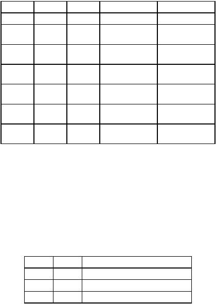
Table 3-1. Data Strobe Control of Data Bus
|
|
R/ |
D8–D15 |
D0–D7 |
High |
High |
— |
No Valid Data |
No Valid Data |
Low |
Low |
High |
Valid Data Bits |
Valid Data Bits |
|
|
|
15–8 |
7–0 |
High |
Low |
High |
No Valid Data |
Valid Data Bits |
|
|
|
|
7–0 |
Low |
High |
High |
Valid Data Bus |
No Valid Data |
|
|
|
15–8 |
|
Low |
Low |
Low |
Valid Data Bits |
Valid Data Bits |
|
|
|
15–8 |
7–0 |
High |
Low |
Low |
Valid Data Bits |
Valid Data Bits |
|
|
|
7–0* |
7–0 |
Low |
High |
Low |
Valid Data Bits |
Valid Data Bits |
|
|
|
15–8 |
15–8* |
*These conditions are a result of current implementation and may not appear on future devices.
Data Strobe ( ) (MC68008)
This three-state signal and R/W control the flow of data on the data bus of the MC68008. Table 3-2 lists the combinations of these signals and the corresponding data on the bus. When the R/W line is high, the processor reads from the data bus. When the R/W line is low, the processor drives the data bus.
|
Table 3-2. Data Strobe Control |
|
|
of Data Bus (MC68008) |
|
|
R/ |
D0–D7 |
1 |
— |
No Valid Data |
0 |
1 |
Valid Data Bits 7–0 (Read Cycle) |
0 |
0 |
Valid Data Bits 7–0 (Write Cycle) |
Data Transfer Acknowledge ( |
). |
|
This input signal indicates the completion of the data transfer. When the processor recognizes DTACK during a read cycle, data is latched, and the bus cycle is terminated.
When DTACK is recognized during a write cycle, the bus cycle is terminated.
3.4 BUS ARBITRATION CONTROL
The bus request, bus grant, and bus grant acknowledge signals form a bus arbitration circuit to determine which device becomes the bus master device. In the 48-pin version of the MC68008 and MC68EC000, no pin is available for the bus grant acknowledge signal; this microprocessor uses a two-wire bus arbitration scheme. All M68000 processors can use two-wire bus arbitration.
MOTOROLA |
M68000 8-/16-/32-BIT MICROPROCESSORS USER'S MANUAL |
3-5 |
Bus Request ( ).
This input can be wire-ORed with bus request signals from all other devices that could be bus masters. This signal indicates to the processor that some other device needs to become the bus master. Bus requests can be issued at any time during a cycle or between cycles.
Bus Grant ( ).
This output signal indicates to all other potential bus master devices that the processor will relinquish bus control at the end of the current bus cycle.
Bus Grant Acknowledge ( |
). |
This input indicates that some other device has become the bus master. This signal should not be asserted until the following conditions are met:
1.A bus grant has been received.
2.Address strobe is inactive, which indicates that the microprocessor is not using the bus.
3.Data transfer acknowledge is inactive, which indicates that neither memory nor peripherals are using the bus.
4.Bus grant acknowledge is inactive, which indicates that no other device is still claiming bus mastership.
The 48-pin version of the MC68008 has no pin available for the bus grant acknowledge signal and uses a two-wire bus arbitration scheme instead. If another device in a system supplies a bus grant acknowledge signal, the bus request input signal to the processor should be asserted when either the bus request or the bus grant acknowledge from that device is asserted.
3.5 INTERRUPT CONTROL ( , |
, |
) |
These input signals indicate the encoded priority level of the device requesting an interrupt. Level seven, which cannot be masked, has the highest priority; level zero indicates that no interrupts are requested. IPL0 is the least significant bit of the encoded level, and IPL2 is the most significant bit. For each interrupt request, these signals must remain asserted until the processor signals interrupt acknowledge (FC2–FC0 and A19– A16 high) for that request to ensure that the interrupt is recognized.
NOTE
The 48-pin version of the MC68008 has only two interrupt control signals: IPL0/IPL2 and IPL1. IPL0/IPL2 is internally connected to both IPL0 and IPL2, which provides four interrupt priority levels: levels 0, 2, 5, and 7. In all other respects, the interrupt priority levels in this version of the MC68008 are identical to those levels in the other microprocessors described in this manual.
3-6 |
M68000 8-/16-/32-BIT MICROPROCESSORS USER'S MANUAL |
MOTOROLA |