

ADDR |
|
11 |
|
AS |
|
20A |
|
R/W |
|
|
22 |
UDS/LDS |
|
55 |
26 |
DATA |
|
DTACK |
|
28 |
29 |
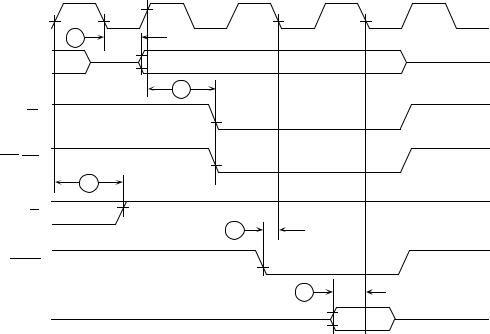
Figure 5-34. Pseudo-Asynchronous Write Cycle
In the MC68010, the BERR signal can be delayed after the assertion of DTACK. Specification #48 is the maximum time between assertion of DTACK and assertion of BERR. If this maximum delay is exceeded, operation of the processor may be erratic.
5.8 SYNCHRONOUS OPERATION
In some systems, external devices use the system clock to generate DTACK and other asynchronous input signals. This synchronous operation provides a closely coupled design with maximum performance, appropriate for frequently accessed parts of the system. For example, memory can operate in the synchronous mode, but peripheral devices operate asynchronously. For a synchronous device, the designer uses explicit timing information shown in Section 10 Electrical Characteristics. These specifications define the state of all bus signals relative to a specific state of the processor clock.
The standard M68000 bus cycle consists of four clock periods (eight bus cycle states) and, optionally, an integral number of clock cycles inserted as wait states. Wait states are inserted as required to allow sufficient response time for the external device. The following state-by-state description of the bus cycle differs from those descriptions in 5.1.1 READ CYCLE and 5.1.2 WRITE CYCLE by including information about the important timing parameters that apply in the bus cycle states.
STATE 0 The bus cycle starts in S0, during which the clock is high. At the rising edge of S0, the function code for the access is driven externally. Parameter #6A defines the delay from this rising edge until the function codes are valid.
Also, the R/W signal is driven high; parameter #18 defines the delay from the same rising edge to the transition of R/W . The minimum value for parameter #18 applies to a read cycle preceded by a write cycle; this value
MOTOROLA |
M68000 8-/16-/32-BIT MICROPROCESSORS USER'S MANUAL |
5-35 |
is the maximum hold time for a low on R/W beyond the initiation of the read cycle.
STATE 1 Entering S1, a low period of the clock, the address of the accessed device is driven externally with an assertion delay defined by parameter #6.
STATE 2 On the rising edge of S2, a high period of the clock, AS is asserted. During a read cycle, UDS, LDS, and/or DS is also asserted at this time. Parameter
#9 defines the assertion delay for these signals. For a write cycle, the R/W signal is driven low with a delay defined by parameter #20.
STATE 3 On the falling edge of the clock entering S3, the data bus is driven out of the high-impedance state with the data being written to the accessed device (in a write cycle). Parameter #23 specifies the data assertion delay. In a read cycle, no signal is altered in S3.
STATE 4 Entering the high clock period of S4, UDS, LDS, and/or DS is asserted
(during a write cycle) on the rising edge of the clock. As in S2 for a read cycle, parameter #9 defines the assertion delay from the rising edge of S4 for UDS, LDS, and/or DS. In a read cycle, no signal is altered by the processor during S4.
Until the falling edge of the clock at the end of S4 (beginning of S5), no response from any external device except RESET is acknowledged by the processor. If either DTACK or BERR is asserted before the falling edge of S4 and satisfies the input setup time defined by parameter #47, the processor enters S5 and the bus cycle continues. If either DTACK or BERR is asserted but without meeting the setup time defined by parameter #47, the processor may recognize the signal and continue the bus cycle; the result is unpredictable. If neither DTACK nor BERR is asserted before the next rise of clock, the bus cycle remains in S4, and wait states (complete clock cycles) are inserted until one of the bus cycle termination is met.
STATE 5 S5 is a low period of the clock, during which the processor does not alter any signal.
STATE 6 S6 is a high period of the clock, during which data for a read operation is set up relative to the falling edge (entering S7). Parameter #27 defines the minimum period by which the data must precede the falling edge. For a write operation, the processor changes no signal during S6.
STATE 7 On the falling edge of the clock entering S7, the processor latches data and negates AS and UDS, LDS, and/or DS during a read cycle. The hold time for these strobes from this falling edge is specified by parameter #12.
The hold time for data relative to the negation of AS and UDS, LDS, and/or
DS is specified by parameter #29. For a write cycle, only AS and UDS, LDS, and/or DS are negated; timing parameter #12 also applies.
5-36 |
M68000 8-/16-/32-BIT MICROPROCESSORS USER'S MANUAL |
MOTOROLA |
On the rising edge of the clock, at the end of S7 (which may be the start of
S0 for the next bus cycle), the processor places the address bus in the high-impedance state. During a write cycle, the processor also places the data bus in the high-impedance state and drives R/W high. External logic circuitry should respond to the negation of the AS and UDS, LDS, and/or DS by negating DTACK and/or BERR. Parameter #28 is the hold time for
DTACK, and parameter #30 is the hold time for BERR.
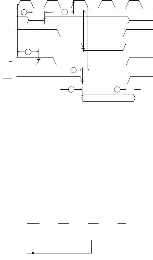
Figure 5-35 shows a synchronous read cycle and the important timing parameters that apply. The timing for a synchronous read cycle, including relevant timing parameters, is shown in Figure 5-36.
S0 |
S1 |
S2 |
S3 |
S4 |
S5 |
S6 |
S7 |
S0 |
CLOCK |
|
|
|
|
|
|
|
|
6 |
|
|
|
|
|
|
|
|
ADDR |
|
|
|
|
|
|
|
|
|
|
|
9 |
|
|
|
|
|
AS |
|
|
|
|
|
|
|
|
UDS/LDS |
|
|
|
|
|
|
|
|
18 |
|
|
|
|
|
|
|
|
R/W |
|
|
|
|
|
|
|
|
|
|
|
|
47 |
|
|
|
|
DTACK |
|
|
|
|
|
|
|
|
|
|
|
|
|
27 |
|
|
|
DATA |
|
|
|
|
|
|
|
|
Figure 5-35. Synchronous Read Cycle
MOTOROLA |
M68000 8-/16-/32-BIT MICROPROCESSORS USER'S MANUAL |
5-37 |
S0 |
S1 |
S2 |
S3 |
S4 |
S5 |
S6 |
S7 |
S0 |
CLOCK |
|
|
|
|
|
|
|
|
6 |
|
|
9. |
|
|
|
|
|
ADDR |
|
|
|
|
|
|
|
|
AS |
|
|
|
|
|
|
|
|
UDS/LDS |
|
|
|
|
|
|
|
|
18 |
|
|
|
|
|
|
|
|
R/W |
|
|
|
|
|
|
|
|
|
|
|
|
47 |
|
|
|
|
DTACK |
|
|
|
|
|
|
|
|
|
|
|
|
23 |
|
|
53 |
|
DATA |
|
|
|
|
|
|
|
|
Figure 5-36. Synchronous Write Cycle
A key consideration when designing in a synchronous environment is the timing for the assertion of DTACK and BERR by an external device. To properly use external inputs, the processor must synchronize these signals to the internal clock. The processor must sample the external signal, which has no defined phase relationship to the CPU clock, which may be changing at sampling time, and must determine whether to consider the signal high or low during the succeeding clock period. Successful synchronization requires that the internal machine receives a valid logic level (not a metastable signal), whether the input is high, low, or in transition. Metastable signals propagating through synchronous machines can produce unpredictable operation.
Figure 5-37 is a conceptual representation of the input synchronizers used by the M68000 Family processors. The input latches allow the input to propagate through to the output when E is high. When low, E latches the input. The three latches require one cycle of CLK to synchronize an external signal. The high-gain characteristics of the devices comprising the latches quickly resolve a marginal signal into a valid state.
EXT |
D |
Q |
|
D |
Q |
|
D |
Q |
INT |
SIGNAL |
|
|
SIGNAL |
||||||
|
|
|
|
|
|
|
|
||
|
G |
|
|
G |
|
|
G |
|
|
|
|
|
|
|
|
|
|
|
|
CLK
CLK
Figure 5-37. Input Synchronizers
5-38 |
M68000 8-/16-/32-BIT MICROPROCESSORS USER'S MANUAL |
MOTOROLA |
Parameter #47 of Section 10 Electrical Characteristics is the asynchronous input setup time. Signals that meet parameter #47 are guaranteed to be recognized at the next falling edge of the system clock. However, signals that do not meet parameter #47 are not guaranteed to be recognized. In addition, if DTACK is recognized on a falling edge, valid data is latched into the processor (during a read cycle) on the next falling edge, provided the data meets the setup time required (parameter #27). When parameter #27 has been met, parameter #31 may be ignored. If DTACK is asserted with the required setup time before the falling edge of S4, no wait states are incurred, and the bus cycle runs at its maximum speed of four clock periods.
The late BERR in an MC68010 that is operating in a synchronous mode must meet setup time parameter #27A. That is, when BERR is asserted after DTACK, BERR must be asserted before the falling edge of the clock, one clock cycle after DTACK is recognized. Violating this requirement may cause the MC68010 to operate erratically.
MOTOROLA |
M68000 8-/16-/32-BIT MICROPROCESSORS USER'S MANUAL |
5-39 |