


STATE 12 The write portion of the cycle starts in S12. The valid function codes on
FC2–FC0, the address bus lines, AS, and R/W remain unaltered.
STATE 13 During S13, no bus signals are altered.
STATE 14 On the rising edge of S14, the processor drives R/W low.
STATE 15 During S15, the data bus is driven out of the high-impedance state as the data to be written are placed on the bus.
STATE 16 At the rising edge of S16, the processor asserts U D S or L D S . The processor waits for DTACK or BERR or VPA, an M6800 peripheral signal. When VPA is asserted during S16, the cycle becomes a peripheral cycle (refer to Appendix B M6800 Peripheral Interface). If neither termination signal is asserted before the falling edge at the close of S16, the processor inserts wait states (full clock cycles) until either DTACK or BERR is asserted.
STATE 17 During S17, no bus signals are altered.
STATE 18 During S18, no bus signals are altered.
STATE 19 On the falling edge of the clock entering S19, the processor negates AS, UDS, and LDS. As the clock rises at the end of S19, the processor places the address and data buses in the high-impedance state, and drives R/W high. The device negates DTACK or BERR at this time.
5.1.4 CPU Space Cycle
A CPU space cycle, indicated when the function codes are all high, is a special processor cycle. Bits A16–A19 of the address bus identify eight types of CPU space cycles. Only the interrupt acknowledge cycle, in which A16–A19 are high, applies to all the microprocessors described in this manual. The MC68010 defines an additional type of CPU space cycle, the breakpoint acknowledge cycle, in which A16–A19 are all low. Other configurations of A16–A19 are reserved by Motorola to define other types of CPU cycles used in other M68000 Family microprocessors. Figure 5-10 shows the encoding of CPU space addresses.
|
FUNCTION |
|
|
|
|
|
|
|
|
|
|
|
ADDRESS BUS |
|
|
|
|
|
|
|
|
|
|
|
|
|
|
|
|
||||||||
|
2 |
CODE |
0 |
|
31 |
|
|
|
|
|
|
|
23 |
|
|
|
19 |
|
|
16 |
|
|
|
|
|
|
|
|
|
|
|
|
|
|
|
|
0 |
BREAKPOINT |
|
|
|
|
|
|
|
|
|
|
|
|
|
|
|
|
|
|
|
|
|
|
|
|
|
|
|
|
|
|
|||||||
1 |
1 |
1 |
|
0 |
0 |
0 |
0 |
0 |
0 |
0 |
0 |
0 |
0 |
0 |
0 |
0 |
0 |
0 |
0 |
|
0 |
0 |
0 |
0 |
0 |
0 |
0 |
0 |
0 |
0 |
0 |
0 |
0 |
0 |
0 |
0 |
|
ACKNOWLEDGE |
|
|
|||||||||||||||||||||||||||||||||||
|
|
|
|
|
|
|
|
|
|
|
|
|
|
|
|
|
|
|
|
|
|
|
|
|
|
|
|
|
|
|
|
|
|
|
|
|
|
|
|
|
|
|
|
|
|
|
|
|
|
|
|
|
|
|
|
|
|
|
|
|
|
|
|
|
|
|
|
|
|
|
|
|
|
|
|
(MC68010 only) |
|
|
|
|
|
|
|
|
|
|
|
|
|
|
|
|
|
|
|
|
|
|
|
|
|
|
|
|
|
|
|
|
|
|
|
|
|
INTERRUPT |
|
|
|
|
31 |
|
|
|
|
|
|
|
|
|
|
|
|
|
|
|
|
|
|
|
|
|
|
|
|
|
|
|
|
3 |
|
1 |
0 |
1 |
1 |
1 |
|
1 |
1 |
1 |
1 |
1 |
1 |
1 |
1 |
1 |
1 |
1 |
1 |
1 |
1 |
1 |
1 |
|
1 |
1 |
1 |
1 |
1 |
1 |
1 |
1 |
1 |
1 |
1 |
1 |
LEVEL |
1 |
|||
ACKNOWLEDGE |
|
|
|||||||||||||||||||||||||||||||||||
|
|
|
|
|
|
|
|
|
|
|
|
|
|
|
|
|
|
|
|
|
|
|
|
|
|
|
|
|
|
|
|
|
|
|
|
|
|
|
|
|
|
|
|
|
|
|
|
|
|
|
|
|
|
|
|
|
|
|
|
|
|
|
|
|
|
|
|
|
|
|
|
|
|
|
|
|
|
|
|
|
|
|
|
|
|
|
|
|
|
|
|
|
|
|
|
|
|
|
|
|
|
|
|
|
|
|
|
|
|
|
|
|
|
|
|
|
|
|
|
|
|
|
|
|
|
|
|
|
|
|
|
|
|
|
|
|
|
|
|
|
|
|
|
|
|
|
|
|
|
|
|
CPU SPACE
TYPE FIELD
Figure 5-10. CPU Space Address Encoding
MOTOROLA |
M68000 8-/16-/32-BIT MICROPROCESSORS USER'S MANUAL |
5-9 |
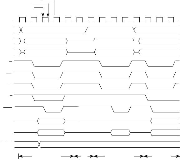
The interrupt acknowledge cycle places the level of the interrupt being acknowledged on address bits A3–A1 and drives all other address lines high. The interrupt acknowledge cycle reads a vector number when the interrupting device places a vector number on the data bus and asserts DTACK to acknowledge the cycle.
The timing diagram for an interrupt acknowledge cycle is shown in Figure 5-11.
Alternately, the interrupt acknowledge cycle can be autovectored. The interrupt acknowledge cycle is the same, except the interrupting device asserts VPA instead of DTACK. For an autovectored interrupt, the vector number used is $18 plus the interrupt level. This is generated internally by the microprocessor when VPA (or AVEC) is asserted on an interrupt acknowledge cycle. DTACK and V P A (AVEC) should never be simultaneously asserted.
IPL2–IPL0 VALID INTERNALLY
IPL2–IPL0 SAMPLED
IPL2–IPL0 TRANSITION
S0 S1 S2 S3 S4 S5 S6 S7 S0 S1 S2 S3 S4 S5 S6 S7 S0 S1 S2 S3 S4 w w w w S5 S6
CLK
FC2–FC0
A23–A4
A3–A1
AS
UDS*
LDS
R/W
DTACK
D15–D8
D7–D0
IPL2–IPL0
LAST BUS CYCLE OF INSTRUCTION |
STACK |
IACK CYCLE |
STACK AND |
(READ OR WRITE) |
PCL |
(VECTOR NUMBER |
VECTOR |
|
(SSP) |
ACQUISITION) |
FETCH |
*Although a vector number is one byte, both data strobes are asserted due to the microcode used for exception processing. The processor does not recognize anything on data lines D8 through D15 at this time.
Figure 5-11. Interrupt Acknowledge Cycle Timing Diagram
5-10 |
M68000 8-/16-/32-BIT MICROPROCESSORS USER'S MANUAL |
MOTOROLA |