

chapter7_pub.fm Page 270 Wednesday, November 22, 2000 8:41 AM
C H A P T E R
7
D E S I G N I N G S E Q U E N T I A L L O G I C
C I R C U I T S
Implementation techniques for flip-flops, latches, oscillators, pulse generators, and Schmitt triggers
n
Static versus dynamic realization
n
Choosing clocking strategies
7.1Introduction
7.2Timing Metrics for Sequential Circuits
7.3Classification of Memory Elements
7.4Static Latches and Registers
7.4.1The Bistability Principle 7.4.2SR Flip-Flops 7.4.3Multiplexer Based Latches
7.4.4Master-Slave Based Edge Triggered Register
7.4.5Non-ideal clock signals 7.4.6Low-Voltage Static Latches
7.5Dynamic Latches and Registers
7.5.1Dynamic Transmission-Gate Based Edge-triggred Registers
7.5.2C2MOS Dynamic Register: A Clock Skew Insensitive Approach
7.5.3True Single-Phase Clocked Register (TSPCR)
7.6Pulse Registers
6.4.2The C2MOS Latch
7.8.2NORA-CMOS—A Logic Style for Pipelined Structures
7.5.3True Single-Phase Clocked Register (TSPCR)
7.7Sense-Amplifier Based Registers
7.8Pipelining: An approach to optimize sequential
circuits
270

chapter7_pub.fm Page 271 Wednesday, November 22, 2000 8:41 AM
Section |
271 |
7.8.1Latchvs. Register-Based Pipelines 7.8.2NORA-CMOS—A Logic Style for Pipelined Structures
7.9Non-Bistable Sequential Circuits 7.9.1The Schmitt Trigger 7.9.2Monostable Sequential Circuits 7.9.3Astable Circuits
7.10Perspective: Choosing a Clocking Strategy
7.11Summary
7.12To Probe Further
7.13Exercises and Design Problems
chapter7_pub.fm Page 272 Wednesday, November 22, 2000 8:41 AM
272 |
DESIGNING SEQUENTIAL LOGIC CIRCUITS |
Chapter 7 |
7.1Introduction
Combinational logic circuits that were described earlier have the property that the output of a logic block is only a function of the current input values, assuming that enough time has elapsed for the logic gates to settle. Yet virtually all useful systems require storage of state information, leading to another class of circuits called sequential logic circuits. In these circuits, the output not only depends upon the current values of the inputs, but also upon preceding input values. In other words, a sequential circuit remembers some of the past history of the system—it has memory.
Figure 7.1 shows a block diagram of a generic finite state machine (FSM) that consists of combinational logic and registers that hold the system state. The system depicted here belongs to the class of synchronous sequential systems, in which all registers are under control of a single global clock. The outputs of the FSM are a function of the current
Inputs and the Current State. The Next State is determined based on the Current State and the current Inputs and is fed to the inputs of registers. On the rising edge of the clock, the Next State bits are copied to the outputs of the registers (after some propagation delay), and a new cycle begins. The register then ignores changes in the input signals until the next rising edge. In general, registers can be positive edge-triggered (where the input data is copied on the positive edge) or negative edge-triggered (where the input data is copied on the negative edge of the clock, as is indicated by a small circle at the clock input).
Inputs |
|
|
|
|
COMBINATIONAL |
|
|
|
Outputs |
|||||||||
|
|
|
|
|
|
|||||||||||||
|
|
|
|
|
|
|
|
|
||||||||||
Current State |
|
|
|
|
|
|
|
LOGIC |
|
|||||||||
|
|
|
|
|
|
|
|
|
|
|
Next State |
|||||||
|
|
|
|
|
|
|
|
|
|
|
|
|
|
|||||
|
|
|
|
|
|
|
Registers |
|
|
|
|
|||||||
|
|
|
|
|
|
|
|
|
|
|
|
|||||||
|
|
|
|
|
|
|
|
|
Q |
|
D |
|
|
|
|
|
||
|
|
|
|
|
|
|||||||||||||
|
|
|
|
|
|
|
|
|
|
|
|
|
|
|
||||
|
|
|
|
|
|
|
|
|
|
|
|
|
|
|
|
|
|
|
|
|
|
|
|
|
|
|
|
|
|
|
|
|
|
|
|
|
|
CLK
Figure 7.1 Block diagram of a finite state machine using positive edge-triggered registers.
This chapter discusses the CMOS implementation of the most important sequential building blocks. A variety of choices in sequential primitives and clocking methodologies exist; making the correct selection is getting increasingly important in modern digital circuits, and can have a great impact on performance, power, and/or design complexity. Before embarking on a detailed discussion on the various design options, a revision of the design metrics, and a classification of the sequential elements is necessary.
7.2Timing Metrics for Sequential Circuits
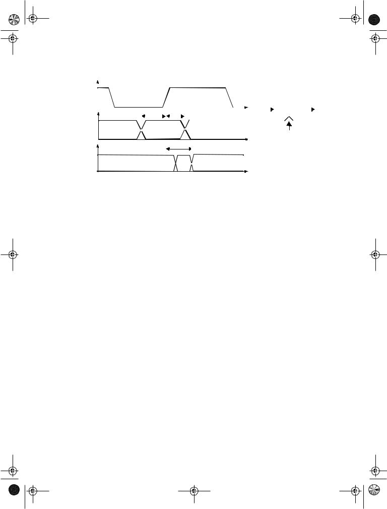
There are three important timing parameters associated with a register as illustrated in Figure 7.2. The set-up time (tsu) is the time that the data inputs (D input) must be valid before the clock transition (this is, the 0 to 1 transition for a positive edge-triggered register). The hold time (thold) is the time the data input must remain valid after the clock edge. Assum-
chapter7_pub.fm Page 273 Wednesday, November 22, 2000 8:41 AM
Section 7.3 |
Classification of Memory Elements |
|
|
|
|
|
273 |
|||||||||
CLK |
|
|
|
|
|
|
|
|
|
|
|
|
|
|
|
|
|
|
|
|
|
|
|
|
|
|
|
|
|
|
|
|
|
|
|
|
|
|
|
|
|
|
t |
Register |
|
|
||||
|
|
|
|
|
|
|
|
|
|
|
|
|
||||
|
|
|
|
|
|
|
|
|
|
|
|
|
D |
Q |
|
|
|
|
tsu |
|
thold |
|
|
|
|
||||||||
|
|
|
|
|
|
|
|
|
||||||||
|
|
|
|
|
|
|
|
|
|
|
|
|
|
|
|
|
D |
DATA |
|
|
STABLE |
t |
|
|
|
|
tc-q |
|
Q |
DATA |
|
|
STABLE |
t |
CLK
Figure 7.2 Definition of set-up time, hold time, and propagation delay of a synchronous register.
ing that the set-up and hold-times are met, the data at the D input is copied to the Q output after a worst-case propagation delay (with reference to the clock edge) denoted by tc-q.
Given the timing information for the registers and the combination logic, some sys- tem-level timing constraints can be derived. Assume that the worst-case propagation
delay of the logic equals tplogic, while its minimum delay (also called the contamination delay) is tcd. The minimum clock period T, required for proper operation of the sequential
circuit is given by
T ≥ tc-q + tplog ic + tsu |
(7.1) |
The hold time of the register imposes an extra constraint for proper operation, |
|
tcdregister + tcdlogic ≥ thold |
(7.2) |
where tcdregister is the minimum propagation delay (or contamination delay) of the register. As seen from Eq. (7.1), it is important to minimize the values of the timing parame-
ters associated with the register, as these directly affect the rate at which a sequential circuit can be clocked. In fact, modern high-performance systems are characterized by a very-low logic depth, and the register propagation delay and set-up times account for a significant portion of the clock period. For example, the DEC Alpha EV6 microprocessor [Gieseke97] has a maximum logic depth of 12 gates, and the register overhead stands for approximately 15% of the clock period. In general, the requirement of Eq. (7.2) is not hard to meet, although it becomes an issue when there is little or no logic between registers, (or when the clocks at different registers are somewhat out of phase due to clock skew, as will be discussed in a later Chapter).
7.3Classification of Memory Elements
Foreground versus Background Memory
At a high level, memory is classified into background and foreground memory. Memory that is embedded into logic is foreground memory, and is most often organized as individual registers of register banks. Large amounts of centralized memory core are referred to as background memory. Background memory, discussed later in this book, achieves
chapter7_pub.fm Page 274 Wednesday, November 22, 2000 8:41 AM
274 |
DESIGNING SEQUENTIAL LOGIC CIRCUITS |
Chapter 7 |
higher area densities through efficient use of array structures and by trading off performance and robustness for size. In this chapter, we focus on foreground memories.
Static versus Dynamic Memory
Memories can be static or dynamic. Static memories preserve the state as long as the power is turned on. Static memories are built using positive feedback or regeneration, where the circuit topology consists of intentional connections between the output and the input of a combinational circuit. Static memories are most useful when the register won’t be updated for extended periods of time. An example of such is configuration data, loaded at power-up time. This condition also holds for most processors that use conditional clocking (i.e., gated clocks) where the clock is turned off for unused modules. In that case, there are no guarantees on how frequently the registers will be clocked, and static memories are needed to preserve the state information. Memory based on positive feedback fall under the class of elements called multivibrator circuits. The bistable element, is its most popular representative, but other elements such as monostable and astable circuits are also frequently used.
Dynamic memories store state for a short period of time—on the order of milliseconds. They are based on the principle of temporary charge storage on parasitic capacitors associated with MOS devices. As with dynamic logic discussed earlier, the capacitors have to be refreshed periodically to annihilate charge leakage. Dynamic memories tend to simpler, resulting in significantly higher performance and lower power dissipation. They are most useful in datapath circuits that require high performance levels and are periodically clocked. It is possible to use dynamic circuitry even when circuits are conditionally clocked, if the state can be discarded when a module goes into idle mode.
Latches vs. Registers
A latch is an essential component in the construction of an edge-triggered register. It is level-sensitive circuit that passes the D input to the Q output when the clock signal is high. This latch is said to be in transparent mode. When the clock is low, the input data sampled on the falling edge of the clock is held stable at the output for the entire phase, and the latch is in hold mode. The inputs must be stable for a short period around the falling edge of the clock to meet set-up and hold requirements. A latch operating under the above conditions is a positive latch. Similarly, a negative latch passes the D input to the Q output when the clock signal is low. The signal waveforms for a positive and negative latch are shown in Figure 7.3. A wide variety of static and dynamic implementations exists for the realization of latches.
Contrary to level-sensitive latches, edge-triggered registers only sample the input on a clock transition — 0-to-1 for a positive edge-triggered register, and 1-to-0 for a negative edge-triggered register. They are typically built using the latch primitives of Figure 7.3. A most-often recurring configuration is the master-slave structure that cascades a positive and negative latch. Registers can also be constructed using one-shot generators of the clock signal (“glitch” registers), or using other specialized structures. Examples of these are shown later in this chapter.
chapter7_pub.fm Page 275 Wednesday, November 22, 2000 8:41 AM
Section 7.4 |
|
Static Latches and Registers |
|
|
|
|
|
|
|
|
|
|
|
|
|
|
|
|
275 |
||||||||||||||||||||||
|
|
|
|
|
|
Positive Latch |
|
|
|
|
|
|
|
|
|
|
|
|
Negative Latch |
|
|
|
|
|
|||||||||||||||||
|
|
|
|
|
|
|
|
|
|
|
|
|
|
|
|
|
|
|
|
|
|
|
|
|
|
|
|
|
|
|
|
|
|
|
|
|
|
|
|
|
|
|
In |
|
|
|
|
D |
|
|
Q |
|
|
|
|
|
Out |
|
|
In |
|
|
|
|
D |
|
|
|
Q |
|
|
|
Out |
||||||||||
|
|
|
|
|
|
|
|
|
G |
|
|
|
|
|
|
|
|
|
|
|
|
|
|
|
|
|
|
G |
|
|
|
|
|
|
|
||||||
|
|
|
|
|
|
|
|
|
|
|
CLK |
|
|
|
|
|
|
|
|
|
|
|
|
|
|
|
|
|
|
|
|
|
|
|
|
|
|
||||
clk |
|
|
|
|
|
|
|
|
|
|
|
|
|
|
|
clk |
|
|
|
|
|
|
|
|
|
|
|
|
CLK |
|
|
|
|
|
|||||||
|
|
|
|
|
|
|
|
|
|
|
|
|
|
|
|
|
|
|
|
|
|
|
|
|
|
|
|
|
|
|
|
||||||||||
|
|
|
|
|
|
|
|
|
|
|
|
|
|
|
|
|
|
|
|
|
|
|
|
|
|
|
|
|
|
|
|
||||||||||
|
|
|
|
|
|
|
|
|
|
|
|
|
|
|
|
|
|
|
|
|
|
|
|
|
|
|
|
|
|
|
|
|
|
|
|
|
|||||
|
|
|
|
|
|
|
|
|
|
|
|
|
|
|
|
|
|
|
|
|
|
|
|
|
|
|
|
|
|
|
|
|
|
|
|
|
|||||
|
|
|
|
|
|
|
|
|
|
|
|
|
|
|
|
|
|
|
|
|
|
|
|
|
|
|
|
|
|
|
|
|
|
|
|
|
|
|
|
||
|
|
|
|
|
|
|
|
|
|
|
|
|
|
|
|
|
|
|
|
|
|
|
|
|
|
|
|
|
|
|
|
|
|
|
|
|
|
|
|
||
|
|
|
|
|
|
|
|
|
|
|
|
|
|
|
|
|
|
|
|
|
|
|
|
|
|
|
|
|
|
|
|
|
|
|
|
|
|
|
|
|
|
In |
|
|
|
|
|
|
|
|
|
|
|
|
|
|
|
|
|
|
|
|
In |
|
|
|
|
|
|
|
|
|
|
|
|
|
|
|
|
|
|||
|
|
|
|
|
|
|
|
|
|
|
|
|
|
|
|
|
|
|
|
|
|
|
|
|
|
|
|
|
|
|
|
|
|
|
|
|
|||||
|
|
|
|
|
|
|
|
|
|
|
|
|
|
|
|
|
|
|
|
|
|
|
|
|
|
|
|
|
|
|
|
|
|
|
|
|
|
|
|
|
|
|
|
|
|
|
|
|
|
|
|
|
|
|
|
|
|
|
|
|
|
|
|
|
|
|
|
|
|
|
|
|
|
|
|
|
|
|
|
|
|
|
|
Out |
|
|
|
|
|
|
|
|
|
|
|
|
|
|
|
|
|
|
|
|
Out |
|
|
|
|
|
|
|
|
|
|
|
|
|
|
|
|
|
|||
|
|
|
|
|
|
|
|
|
|
|
|
|
|
|
|
|
|
|
|
|
|
|
|
|
|
|
|
|
|
|
|
|
|
||||||||
|
|
Out |
|
|
|
Out |
|
|
|
|
|
|
Out |
|
Out |
|
|
|
|
|
|
|
|
|
|
|
|||||||||||||||
|
|
stable |
|
|
follows In |
|
|
|
|
|
|
stable |
follows In |
|
|
|
|
|
|
|
|
|
|
|
|||||||||||||||||
Figure 7.3 Timing of positive and negative latches.
7.4Static Latches and Registers
7.4.1The Bistability Principle
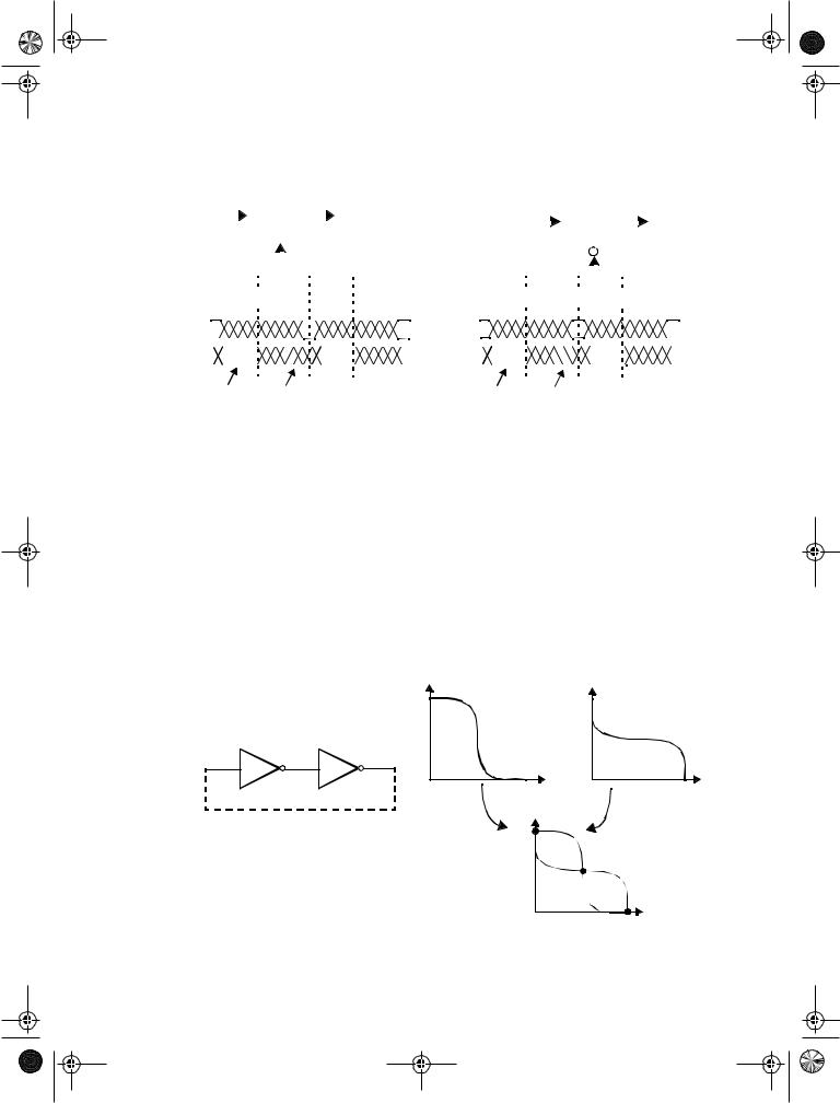
Static memories use positive feedback to create a bistable circuit — a circuit having two stable states that represent 0 and 1. The basic idea is shown in Figure 7.4a, which shows two inverters connected in cascade along with a voltage-transfer characteristic typical of such a circuit. Also plotted are the VTCs of the first inverter, that is, Vo1 versus Vi1, and the second inverter (Vo2 versus Vo1). The latter plot is rotated to accentuate that Vi2 = Vo1. Assume now that the output of the second inverter Vo2 is connected to the input of the first Vi1, as shown by the dotted lines in Figure 7.4a. The resulting circuit has only three possi-
|
|
o1 |
o1 |
|
|
V |
V |
|
|
|
= |
|
|
|
i2 |
|
|
|
V |
Vi1 |
Vo1 = Vi2 |
V |
|
|
|
o2 |
|
|
|
Vi1 |
Vo2 |
|
Vo2 = Vi1 |
o1 |
A |
|
(a) |
= V |
|
|
i2 |
|
|
|
|
|
|
|
|
V |
C |
|
|
|
|
Figure 7.4 Two cascaded inverters (a) |
B |
||
and their VTCs (b). |
|
||
|
Vi1 = Vo2 |
||
|
|
|
|
(b)
chapter7_pub.fm Page 276 Wednesday, November 22, 2000 8:41 AM
276 |
DESIGNING SEQUENTIAL LOGIC CIRCUITS |
Chapter 7 |
ble operation points (A, B, and C), as demonstrated on the combined VTC. The following important conjecture is easily proven to be valid:
Under the condition that the gain of the inverter in the transient region is larger than 1, only A and B are stable operation points, and C is a metastable operation point.
Suppose that the cross-coupled inverter pair is biased at point C. A small deviation from this bias point, possibly caused by noise, is amplified and regenerated around the circuit loop. This is a consequence of the gain around the loop being larger than 1. The effect is demonstrated in Figure 7.5a. A small deviation δ is applied to Vi1 (biased in C). This deviation is amplified by the gain of the inverter. The enlarged divergence is applied to the second inverter and amplified once more. The bias point moves away from C until one of the operation points A or B is reached. In conclusion, C is an unstable operation point. Every deviation (even the smallest one) causes the operation point to run away from its original bias. The chance is indeed very small that the cross-coupled inverter pair is biased at C and stays there. Operation points with this property are termed metastable.
|
A |
|
|
|
A |
|
|
|||||||||
o1 |
|
|
|
|
|
|
|
|
|
|
o1 |
|
|
|
|
|
|
|
|
|
|
|
|
|
|
|
|
|
|
|
|
||
|
|
|
|
|
|
|
|
|
|
|
|
|||||
= V |
|
|
|
|
|
|
|
|
|
|
= V |
|
|
|
|
|
|
|
|
|
|
|
|
|
|
|
|
|
|
|
|
||
i2 |
|
|
|
|
|
|
|
|
|
|
i2 |
|
|
|
|
|
V |
|
|
|
|
|
|
C |
|
B |
V |
|
|
|
C |
||
|
|
|
|
|
|
|
|
|
|
|||||||
|
|
|
|
|
|
|
|
|
|
|
|
|||||
|
|
|
|
|
|
|
|
|
|
|
|
|||||
|
|
|
|
|
|
|
|
|
|
|
|
|||||
|
|
|
|
|
|
|
|
|
|
|
|
|||||
|
|
|
|
|
|
|
|
|
|
|
|
|
|
|
B |
|
|
|
|
|
|
|
|
|
|
|
|
|
|
|
|
||
|
|
|
|
|
|
|
|
|
|
|
|
|
|
|
||
|
|
|
|
|
|
|
|
|
|
|
|
|
|
|
||
|
|
|
|
|
|
|
|
|
|
|
|
|
|
|
||
|
|
|
|
|
|
|
|
|
|
|
|
|
|
|
||
|
|
|
|
|
|
|
|
|
|
|
|
|
|
|
||
|
|
|
|
|
|
|
|
|
|
|
|
|
|
|
||
|
|
|
|
|
|
|
|
|
|
|
|
|
|
|
|
|
|
|
|
|
|
|
|
|
|
|
|
|
|
||||
|
|
|
|
|
δ |
Vi1 = Vo2 |
|
|
δ |
Vi1 = Vo2 |
||||||
|
|
|
|
|
|
(a) |
|
|
|
|
|
|
(b) |
|||
Figure 7.5 Metastability. |
|
|
|
|
|
|
||||||||||
On the other hand, A and B are stable operation points, as demonstrated in Figure 7.5b. In these points, the loop gain is much smaller than unity. Even a rather large deviation from the operation point is reduced in size and disappears.
Hence the cross-coupling of two inverters results in a bistable circuit, that is, a circuit with two stable states, each corresponding to a logic state. The circuit serves as a memory, storing either a 1 or a 0 (corresponding to positions A and B).
In order to change the stored value, we must be able to bring the circuit from state A to B and vice-versa. Since the precondition for stability is that the loop gain G is smaller than unity, we can achieve this by making A (or B) temporarily unstable by increasing G to a value larger than 1. This is generally done by applying a trigger pulse at Vi1 or Vi2. For instance, assume that the system is in position A (Vi1 = 0, Vi2 = 1). Forcing Vi1 to 1 causes both inverters to be on simultaneously for a short time and the loop gain G to be larger than 1. The positive feedback regenerates the effect of the trigger pulse, and the circuit moves to the other state (B in this case). The width of the trigger pulse need be only a little
chapter7_pub.fm Page 277 Wednesday, November 22, 2000 8:41 AM
Section 7.4 |
Static Latches and Registers |
277 |
larger than the total propagation delay around the circuit loop, which is twice the average propagation delay of the inverters.
In summary, a bistable circuit has two stable states. In absence of any triggering, the circuit remains in a single state (assuming that the power supply remains applied to the circuit), and hence remembers a value. A trigger pulse must be applied to change the state of the circuit. Another common name for a bistable circuit is flip-flop (unfortunately, an edge-triggered register is also referred to as a flip-flop).
7.4.2SR Flip-Flops
The cross-coupled inverter pair shown in the previous section provides an approach to store a binary variable in a stable way. However, extra circuitry must be added to enable control of the memory states. The simplest incarnation accomplishing this is the wellknow SR —or set-reset— flip-flop, an implementation of which is shown in Figure 7.6a. This circuit is similar to the cross-coupled inverter pair with NOR gates replacing the inverters. The second input of the NOR gates is connected to the trigger inputs (S and R), that make it possible to force the outputs Q and Q to a given state. These outputs are complimentary (except for the SR = 11 state). When both S and R are 0, the flip-flop is in a quiescent state and both outputs retain their value (a NOR gate with one of its input being 0 looks like an inverter, and the structure looks like a cross coupled inverter). If a positive (or 1) pulse is applied to the S input, the Q output is forced into the 1 state (with Q going to 0). Vice versa, a 1 pulse on R resets the flip-flop and the Q output goes to 0.
|
|
|
|
|
|
|
|
|
|
|
|
|
|
|
|
|
|
|
|
|
S |
R |
Q |
|
|
|
|
|
S |
|
|
|
|
|
|
|
|
|
|
|
|
|
|
|
|
|
|
|
|
|
Q |
||||||
|
|
|
|
|
|
|
|
|
|
|
|
|
|
|
|
|
|
|
|
|||||||||
|
|
|
|
|
|
|
|
|
|
|
Q |
S |
|
|
|
|
|
|
0 |
|
|
|
|
|
|
|||
|
|
|
|
|
|
|
|
|
|
|
|
|
|
|
Q |
|
0 |
Q |
|
Q |
|
|
||||||
|
|
|
|
|
|
|
|
|
|
|
|
|
|
|
|
|
|
|
1 |
0 |
1 |
0 |
|
|
||||
|
|
|
|
|
|
|
|
|
|
|
|
|
|
|
|
|
|
|
|
|
||||||||
|
|
|
|
|
|
|
|
|
|
|
Q |
R |
Q |
|
|
0 |
1 |
0 |
1 |
|
|
|||||||
|
|
|
|
|
|
|
|
|
|
|
|
|
|
|
|
|
||||||||||||
|
|
|
|
|
|
|
|
|
|
|
|
|
|
|
|
|
|
|
|
|
|
|
|
|
||||
|
|
|
|
|
|
|
|
|
|
|
|
|
|
|
|
|
1 |
1 |
0 |
0 |
|
|
||||||
R |
|
|
|
|
|
|
|
|
|
|
|
|
|
|
|
|
|
|
|
|||||||||
|
|
|
|
|
|
|
|
|
|
|
|
|
|
|
|
|
|
|
|
|
||||||||
|
|
|
|
|
|
|
|
|
|
|
|
|
|
|
|
|
|
|
Forbidden State |
|
|
|
|
|
|
|
||
(a) Schematic diagram |
|
|
|
(b) Logic symbol |
|
|
|
(c) Characteristic table |
||||||||||||||||||||
Figure 7.6 NOR-based SR flip-flop.
These results are summarized in the characteristic table of the flip-flop, shown in Figure 7.6c. The characteristic table is the truth table of the gate and lists the output states as functions of all possible input conditions. When both S and R are high, both Q and Q are forced to zero. Since this does not correspond with our constraint that Q and Q must be complementary, this input mode is considered to be forbidden. An additional problem with this condition is that when the input triggers return to their zero levels, the resulting state of the latch is unpredictable and depends on whatever input is last to go low. Finally, Figure 7.6 shows the schematics symbol of the SR flip-flop.
chapter7_pub.fm Page 278 Wednesday, November 22, 2000 8:41 AM
278 |
DESIGNING SEQUENTIAL LOGIC CIRCUITS |
Chapter 7 |
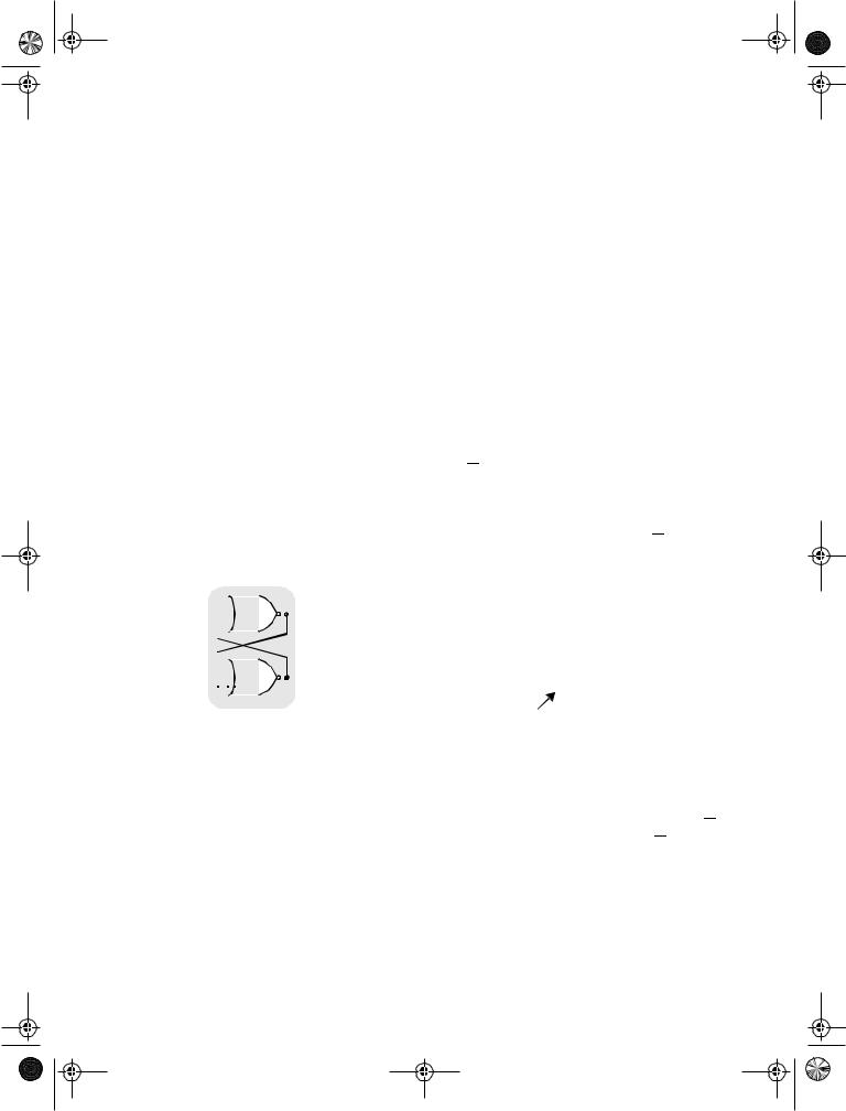
Problem 7.1 SR Flip-Flop Using NAND Gates
An SR flip-flop can also be implemented using a cross-coupled NAND structure as shown in Figure 7.7. Derive the truth table for a such an implementation.
S
Q
Q
R
Figure 7.7 NAND-based SR flip-flop.
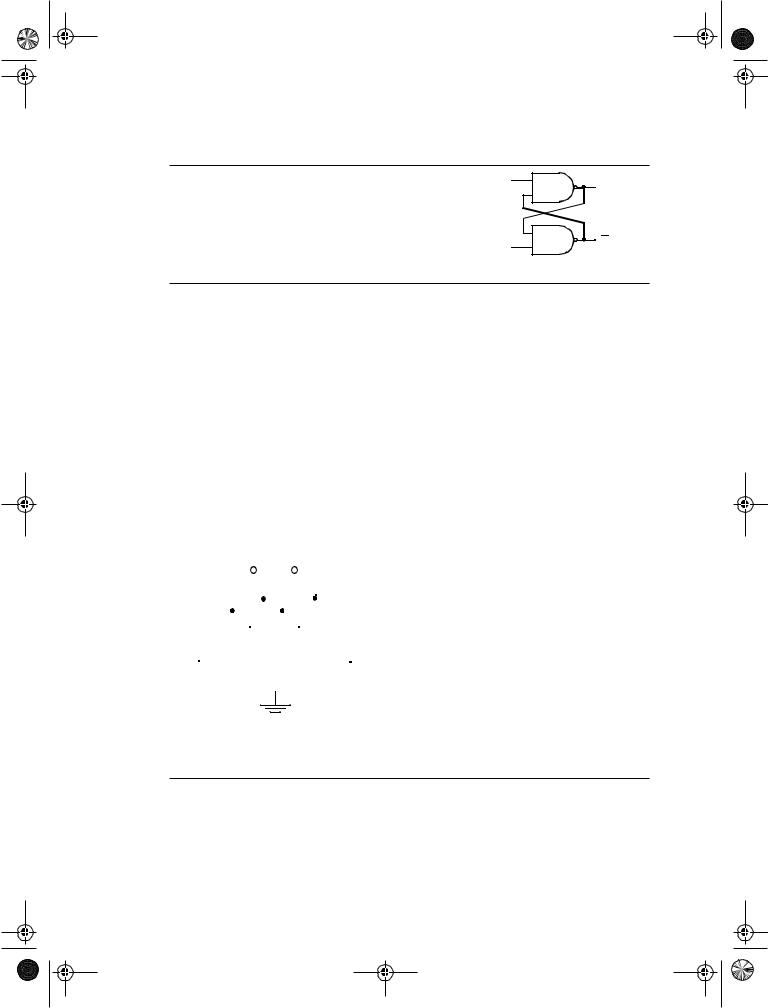
The SR flip-flops discussed so far are asynchronous, and do not require a clock signal. Most systems operate in a synchronous fashion with transition events referenced to a clock. One possible realization of a clocked SR flip-flop— a level-sensitive positive latch— is shown in Figure 7.8. It consists of a cross-coupled inverter pair, plus 4 extra transistors to drive the flip-flop from one state to another and to provide clocked operation. Observe that the number of transistors is identical to the implementation of Figure 7.6, but the circuit has the added feature of being clocked. The drawback of saving some transistors over a fully-complimentary CMOS implementation is that transistor sizing becomes critical in ensuring proper functionality. Consider the case where Q is high and an R pulse is applied. The combination of transistors M4, M7, and M8 forms a ratioed inverter. In order to make the latch switch, we must succeed in bringing Q below the switching threshold of the inverter M1-M2. Once this is achieved, the positive feedback causes the flip-flop to invert states. This requirement forces us to increase the sizes of transistors M5, M6, M7, and M8.
|
|
|
|
|
|
|
|
|
|
VDD |
|
|
|
||||||||
|
|
|
|
|
|
|
|
|
|
|
|
|
|
|
|
|
|
|
|
|
|
|
|
|
|
|
|
|
|
|
|
|
|
|
|
|
|
|
|
|
|
|
|
|
|
|
|
|
|
M2 |
|
|
|
|
|
|
|
M4 |
|
|
|
||||
|
|
|
|
|
|
|
|
|
|
|
|
|
|||||||||
|
|
|
|
|
|
|
|
|
|
|
|
|
|
|
|
Q |
|
|
|
||
|
|
|
|
|
|
|
|
|
|
|
|
|
|
|
|
|
|
|
|||
|
|
|
|
|
Q |
|
|
|
|
|
|
|
|
|
|
|
|
|
|
|
|
|
|
|
|
|
|
|
|
|
|
|
|
|
|
|
|
|
|
|
|||
|
|
|
|
|
|
|
|
|
|
|
|
|
|
|
|
|
|
|
|
|
|
CLK |
|
|
M6 |
|
|
|
|
|
|
|
|
|
M8 |
|
|
CLK |
|||||
|
|
|
|
|
|
M1 |
|
|
|
|
|
|
|
M3 |
|
|
|
|
|||
|
|
|
|
|
|
|
|
|
|
|
|
|
|
|
|
|
|
|
|
|
|
S |
|
|
M5 |
|
|
|
|
|
|
|
|
|
M7 |
|
|
R |
|||||
|
|
|
|
|
|
|
|
|
|
|
|
||||||||||
|
|
|
|
|
|
|
|
|
|
|
|
|
|
|
|
|
|
|
|
|
|
|
|
|
|
|
|
|
|
|
|
|
|
|
|
|
|
|
|
|
|
|
|
Figure 7.8 CMOS clocked SR flip-flop.
The presented flip-flop does not consume any static power. In steady-state, one inverter resides in the high state, while the other one is low. No static paths between VDD and GND can exist except during switching.
Example 7.1 Transistor Sizing of Clocked SR Latch
Assume that the cross-coupled inverter pair is designed such that the inverter threshold VM is located at VDD/2. For a 0.25 m CMOS technology, the following transistor sizes were
selected: (W/L)M1 = (W/L)M3 = (0.5 m/0.25 m), and (W/L)M2 = (W/L)M4 = (1.5 m/0.25 m). Assuming Q = 0, we determine the minimum sizes of M5, M6, M7, and M8 to make the device
switchable.
chapter7_pub.fm Page 279 Wednesday, November 22, 2000 8:41 AM
Section 7.4 |
Static Latches and Registers |
279 |
To switch the latch from the Q = 0 to the Q = 1 state, it is essential that the low level of the ratioed, pseudo-NMOS inverter (M5-M6)-M2 be below the switching threshold of the inverter M3-M4 that equals VDD/2. It is reasonable to assume that as long as VQ > VM, VQ equals 0, and the gate of transistor M2 is grounded. The boundary conditions on the transistor sizes can be derived by equating the currents in the inverter for VQ = VDD / 2, as given in Eq. (7.3) (this ignores channel length modulation). The currents are determined by the saturation current since VSET = VDD = 2.5V and VM = 1.25V. We assume that M5 and M6 have identical sizes and that W/L5-6 is the effective ratio of the series-connected devices. Under this condition, the pull-down network can be modeled by a single transistor M56, whose length is twice the length of the individual devices.
k′n |
W |
( VDD – VTn) VDSAT n – |
VD2SAT n |
= k′p |
|
W |
|
( – VDD – VTp) VDSAT p – |
VD2 SAT p |
|
(7.3) |
---- |
--------2-------- |
|
-L--- |
|
--------2-------- |
|
|||||
|
L |
5 – 6 |
|
|
|
2 |
|
|
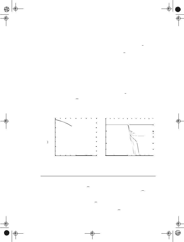
Using the parameters for the 0.25 µ m process, Eq. (7.3) results in the constraint that the effective (W/L)M5-6 ≥ 2.26. This implies that the individual device ratio for M5 or M6 must be larger that approximately 4.5. Figure 7.9a shows the DC plot of VQ as a function of the individual device sizes of M5 and M6. We notice that the individual device ratio of greater than 3
is sufficient to bring the Q voltage to the inverter switching threshold. The difference between the manual analysis and simulation arises due to second order effects such as DIBL and channel length modulation. Figure 7.9b, which shows the transient response for different device sizes. The plot confirms that an individual W/L ratio of greater than 3 is required to overpower the feedback and switch the state of the latch.
|
2.0 |
|
|
|
|
|
|
|
|
|
|
|
|
|
|
(Volts)Q |
1.5 |
|
|
|
|
|
|
1.0 |
|
|
|
|
|
|
|
|
|
|
|
|
|
|
|
|
0.5 |
|
|
|
|
|
|
|
0.02.0 |
2.5 |
3.0 |
3.5 |
|
|
|
|
4.0 |
||||||
|
|
|
|
W/L5and 6 |
|
|
|
(a)
Volts
3 |
|
|
|
|
|
|
|
|
|
|
|
|
|
|
|
|
|
|
|
|
|
|
|
|
|
S |
|
|
|
|
|
|
|
|
|
|
|
|
|
|
|
|||
|
|
|
|
|
|
Q |
|
|
|
|
|
|
|
|
2 |
|
|
|
|
|
|
|
|
|
|
W=0.5 m |
|
||
|
|
|
|
|
|
|
|
|
|
|
|
|
|
|
|
|
|
|
|
|
|
|
|
|
|
W=0.6 m |
|
||
|
|
|
|
|
|
|
|
|
|
|
W=0.7 m |
|
||
1 |
|
|
|
|
|
|
|
|
|
|
W=0.8 m |
|
|
|
|
|
|
|
|
|
|
|
W=1 m |
W=0.9 m |
|
|
|||
0 0 |
|
|
|
|
|
|
|
|
|
|
|
|||
0.2 |
0.4 |
0.6 |
0.8 |
1 |
1.2 |
1.4 |
1.6 |
1.8 |
2 |
|
||||
|
||||||||||||||
|
|
|
|
|
|
|
time (nsec) |
|
|
|
|
|
||
(b)
Figure 7.9 Sizing issues for SR flip-flop. (a) DC output voltage vs. individual pulldown device size of M5 and M6 with W/L2= 1.5 m/.25 m. (b) Transient response shows that M5 and M6 must each have a W/L larger than 3 to swtich the SR flip-flop.
The positive feedback effect makes a manual derivation of propagation delay of the SR latch non-trivial. Some simplifications are therefore necessary. Consider, for instance, the latch of Figure 7.8, where Q and Q are set to 0 and 1, respectively. A pulse is applied at node S, causing the latch to toggle. In the first phase of the transient, node Q is being pulled down by transistors M5 and M6. Since node Q is initially low, the PMOS device M2 is on while M1 is off. The transient response is hence determined by the pseudo-NMOS
inverter formed by (M5-M6) and M2. Once Q reaches the switching threshold of the CMOS inverter M3-M4, this inverter reacts and the positive feedback comes into action, turning
M2 off and M1 on. This accelerates the pulling down of node Q. From this analysis, we can