

Section 6.5 |
Leakage in Low Voltage Systems |
257 |
As with propagation delay, static properties, and switching activity, leakage of logic gates has a strong dependence on the input patterns. The leakage is a function of the circuit topology and the value of inputs. This is due to the fact that VT depends on body bias (VBS) we observe that sub-threshold leakage of a long channel MOS transistor depends on gate drive (VGS) and body bias (VBS). So, in an inverter with IN = 0 the sub-threshold leakage of the inverter will be set by the NMOS transistor with its VGS = VBS = 0 V. In more complex CMOS gates the leakage current will depend on the input vector, for example, one can show (Eq. (6.35)) that the sub-threshold leakage current of a two-input NAND gate will be the least when A = B = 0. Under this condition the intermediate node in will settle to,
VX ≈ Vth ln (1 + n) |
(6.35) |
The NAND gate sub-threshold leakage then will be set by the NMOS transistor with its VGS = VBS = -VX. Clearly, the sub-threshold leakage under this condition will be slightly smaller than that of the inverter or a stand-alone NMOS transistor’s IOFF. This reduction in sub-threshold leakage due to stacked transistors is called the stack effect. Figure 6.69 shows the leakage components for a simple two input NAND gate.
|
|
|
|
|
|
VDD |
||||
A |
|
|
|
|
|
|
|
|
|
|
|
|
P |
1 |
|
|
P2 |
|
|||
|
|
|
|
|
||||||
|
|
|
|
|
|
|||||
|
|
|
|
|
|
|
|
|
|
G |
|
|
|
|
|
|
|
|
|
|
|
|
|
|
|
|
|
|
|
|
|
|
|
A |
|
|
|
|
|
|
|||
|
|
|
|
|
|
|
||||
|
|
|
|
|
|
|
||||
|
|
N |
1 |
|
|
|
||||
|
|
|
|
|
|
|
|
|
||
|
|
|
|
|
|
|
|
VX |
|
|
|
|
|
|
|
|
|||||
|
|
|
|
|
|
|
||||
|
|
|
|
|
|
|
|
|||
|
B |
|
N2 |
|
|
|||||
|
|
|
|
|
|
|
||||
|
|
|
|
|
|
|
|
|
|
|
|
|
|
|
|
|
|
|
|
|
|
|
|
|
|
|
|
|
|
|
|
|
B |
A |
B |
VX |
|
ISUB |
|
|
|
|
|
|
|
|
|
|
|
0 |
0 |
V |
|
ln (1+n) |
IN |
(V |
|
|
= V |
|
= -V |
|
) |
|||
|
th |
GS |
BS |
X |
||||||||||||
|
0 |
1 |
0 |
|
SUB |
(V |
= V |
= 0) |
|
|||||||
|
|
|
IN |
GS |
BS |
|
|
|||||||||
|
|
|
Vdd−VT |
SUB |
|
|
|
|
|
|
|
|||||
|
1 |
0 |
INSUB (VGS = VBS = 0) |
|
|
|||||||||||
|
1 |
1 |
0 |
|
|
2 IP |
|
(V |
SG |
= V = 0) |
||||||
|
|
|
|
|
|
SUB |
|
|
|
SB |
|
|
||||
|
|
|
|
|
|
|
|
|
|
|
|
|
|
|
|
|
Figure 6.69 Sub-threshold leakage reduction due to stack effect in a two-input NAND gate using long channel transistors.
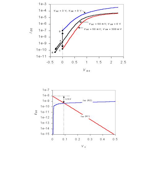
In short channel MOS transistors the sub-threshold leakage current depends not only on the gate drive (VGS) and body bias (VBS), but also depends strongly on the drain voltage (VDS). Threshold voltage of short channel MOS transistors decrease with increase in VDS due to drain induced barrier lowering (DIBL). Typical value for DIBL can range from 20150 mV change in VT per volt change in VDS.
Figure 6.70 shows the decrease in sub-threshold leakage due to (i) decrease in gate drive - point A to B and (ii) increase in body bias - point A to C, similar to long channel MOS transistors. It also illustrates the increase in sub-threshold leakage due to increase in drain voltage - point A to D. Because of this reason the impact of stack effect for leakage reduction will be more significant in short channel MOS transistors. Consider the twoinput NAND gate in Figure 6.69 when both M1 and M2 are off. From the load line in Figure 6.71 we can see that in steady state VX will settle to ~100 mV. So the steady state subthreshold leakage in the NAND gate will be due to VGS = VBS = -100 mV and VDS = VDD - 100 mV which is 20X smaller than that leakage of a stand-alone NMOS transistor with VGS = VBS = 0 mV and VDS = VDD [Ye98]. Because of enhanced stack effect in short channel MOS transistors the sub-threshold leakage in circuits with stacks will be significantly smaller than individual devices. Note that maximum leakage reduction due to stack effect
258 |
DESIGNING COMBINATIONAL LOGIC GATES IN CMOS |
Chapter 6 |
Figure 6.70 Dependence of sub-threshold leakage current on terminal voltages for a typical 0.25 μm NMOS transistor.
Figure 6.71Load line indicating the steady state solution for the intermediate node voltage.
happens when all the transistors in the stack are off and the intermediate node voltage reaches its steady state value. So one can reduce standby leakage in a VLSI system by forcing stack effect in as many gates as possible. Since the intermediate node gets charged or discharged to its steady state value through sub-threshold currents time constant to realize maximum stack effect can be long, depending on the initial node value. A key challenge is to determine the primary input vector that minimizes the leakage effect.
Problem 6.8 Computing VX
Eq. (6.35) represents intermediate node voltage for a two-input NAND with less than 10% error, when A = B = 0. Derive Eq. (6.35) assuming (i) VT and Io of M1 and M2 are approximately equal, (ii) NMOS transistors are identically sized, and (iii) n < 1.5. Explain the tem-

Section 6.6 |
Summary |
259 |
perature dependence of stack effect and leakage reduction due to stack effect using equation (4.5).
6.6Summary
In this chapter, we have extensively analyzed the behavior and performance of combinational CMOS digital circuits with regard to area, speed, and power.
•Static complementary CMOS combines dual pull-down and pull-up networks, only one of which is enabled at any time.
•The performance of a CMOS gate is a strong function of fan-in. Techniques to deal with fan-in include transistor sizing, input reordering, and partitioning. The speed is also a linear function of the fan-out. Extra buffering is needed for large fan-outs.
•The ratioed logic style consists of an active pull-down (up) network connected to a load device. This results in a substantial reduction in gate complexity at the expense of static power consumption and an asymmetrical response. Careful transistor sizing is necessary to maintain sufficient noise margins. The most popular approaches in this class are the pseudo-NMOS techniques and the differential DCVSL, which requires complementary signals.
•Pass-transistor logic implements a logic gate as a simple switch network. This results in very simple implementations for some logic functions. Long cascades of switches are to be avoided due to a quadratic increase in delay with respect to the number of elements in the chain. NMOS-only pass-transistor logic produces even simpler structures, but might suffer from static power consumption and reduced noise margins. This problem can be addressed by adding a level-restoring transistor.
•The operation of dynamic logic is based on the storage of charge on a capacitive node and the conditional discharging of that node as a function of the inputs. This calls for a two-phase scheme, consisting of a precharge followed by an evaluation step. Dynamic logic trades off noise margin for performance. It is sensitive to parasitic effects such as leakage, charge redistribution, and clock feedthrough. Cascading dynamic gates can cause hazards and should be addressed carefully.
•The power consumption of a logic network is strongly related to the switching activity of the network. This activity is a function of the input statistics, the network topology, and the logic style.
•Sources of power consumption such as glitches and short-circuit currents can be minimized by careful circuit design and transistor sizing.
•Power consumption is minimized by reducing the supply voltage, which increases the delay. Trading off area for power is a way to compensate for that performance loss.
260 |
DESIGNING COMBINATIONAL LOGIC GATES IN CMOS |
Chapter 6 |
•Threshold voltage scaling is required for low-voltage operation. Leakage control is critical for low-voltage operation
6.7To Probe Further
The topic of (C)MOS logic styles is treated extensively in the literature. Numerous texts have been devoted to the issue. Some of the most comprehensive treatments can be found in [Glasser85], [Annaratone86], [Elmasry91], [Uyemura92], and [Weste93]. Regarding the intricacies of high-performance design, [Shoji88] offers the most in-depth discussion of the optimization and analysis of digital MOS circuits. The topic of power minimization is relatively new. Excellent reference works are [Chandrakasan95] and [Rabaey95].
Innovations in the MOS logic area are typically published in the proceedings of the ISSCC Conference and the VLSI circuits symposium, as well as the IEEE Journal of Solid State Circuits (especially the November issue).
REFERENCES
[Annaratone86] M. Annaratone, Digital CMOS Circuit Design, Kluwer, 1986.
[Burd94] T. Burd, Low Power CMOS Library Design Methodology, M.S. thesis, University of Cali- fornia—Berkeley, December 1994.
[Chandrakasan92] A. Chandrakasan, S. Sheng, and R. Brodersen, “Low Power CMOS Digital Design,” IEEE Journal of Solid State Circuits, vol. SC-27, no. 4, pp. 1082–1087, April 1992.
[Chandrakasan94] A. Chandrakasan, Low Power Digital CMOS Design, Ph.D. thesis, University of California—Berkeley, Memorandum No. UCB/ERL M94/65, August 1994.
[Chandrakasan95] A. Chandrakasan and R. Brodersen, Low Power Digital CMOS Design, Kluwer, 1995.
[Chu86] K. Chu and D. Pulfrey, “Design Procedures for Differential Cascade Logic,” IEEE Journal of Solid State Circuits, vol. SC-21, no. 6 (Dec. 1986), pp. 1082–1087.
[Dopperpuhl92] D. Dopperpuhl et al., “A 200-MHz 64-b Dual-Issue CMOS Microprocessor,” IEEE Journal of Solid State Circuits, vol. 27, no. 11, pp. 1555–1567, Nov. 1992.
[Elmasry91] M. Elmasry, Ed., Digital MOS Integrated Circuits II, IEEE Press, 1991.
[Friedman84] V. Friedman and S. Liu, “Dynamic Logic CMOS Circuits,” IEEE Journal of Solid State Circuits, vol. SC-19, no. 2, pp. 263–266, April 1984.
[Glasser85] L. Glasser and D. Dopperpuhl, The Design and Analysis of VLSI Circuits, AddisonWesley, 1985.
[Goncalvez83] N. Goncalvez and H. De Man, “NORA: A Racefree Dynamic CMOS Technique for Pipelined Logic Structures,” IEEE Journal of Solid State Circuits, vol. SC-18, no. 3, pp. 261–266, June 1983.
[Heller84] L. Heller et al., “Cascade Voltage Switch Logic: A Differential CMOS Logic Family,”
Proc. IEEE ISSCC Conference, pp. 16–17, February 1984.
[Hodges88] D. Hodges and H. Jackson, Analysis and Design of Digital Integrated Circuits, McGraw-Hill, 1988.
Section 6.7 |
To Probe Further |
261 |
[Krambeck82] R. Krambeck et al., “High-Speed Compact Circuits with CMOS,” IEEE Journal of Solid State Circuits, vol. SC-17, no. 3, pp. 614–619, June 1982.
[Lee86] C. M. Lee and E. Szeto, “Zipper CMOS,” IEEE Circuits and Systems Magazine, pp. 10–16, May 1986.
[Liu93] D. Liu and C. Svensson, “Trading Speed for Low Power by Choice of Supply and Threshold Voltages,” IEEE Journal of Solid State Circuits, vol. SC-28, no 1, pp. 10–17, January 1993.
[Murphy81] B. Murphy and R. Edwards, “A CMOS 32b Single Chip Microprocessor,” Proc. ISCC 81, pp. 230–231, 1981.
[Rabaey95] J. Rabaey and M. Pedram, Low Power Design Methodolgies, Kluwer, 1995. [Radhakrishnan85] D. Radhakrishnan, S. Whittaker, and G. Maki, “Formal Design Procedures for
Pass-Transistor Switching Circuits,” IEEE Journal of Solid State Circuits, vol. SC-20, no. 2, pp. 531–536, April 1985.
[Shimohigashi93] K. Shimohigashi and K. Seki, “Low-Voltage ULSI Design,” IEEE Journal of Solid State Circuits, vol. 28, no. 4, April 1993.
[Shoji88] M. Shoji, CMOS Digital Circuit Technology, Prentice Hall, 1988.
[Uyemura88] J. Uyemura, Fundamentals of MOS Digital Integrated Circuits, Addison-Wesley, 1988.
[Uyemura92] J. Uyemura, Circuit Design for CMOS VLSI, Kluwer, 1992.
[Veendrick84] H. Veendrick, “Short-Circuit Dissipation of Static CMOS Circuitry and Its Impact on the Design of Buffer Circuits,” IEEE Journal of Solid State Circuits, vol. SC-19, no 4, pp. 468–473, August 1984.
[Weste93] N. Weste and K. Eshragian, Principles of CMOS VLSI Design: A Systems Perspective, Addison-Wesley, 1993.
[Yano90] K. Yano et al., “A 3.8 ns CMOS 16 × 16 b Multiplier Using Complimentary PassTransistor Logic,” IEEE Journal of Solid State Circuits, vol. SC-25, no 2, pp. 388–395, April 1990.