

Advancements in rigid-flex circuit board materials, stack-ups, and constructions now allow for a wide variety of advanced design configurations. These options create significant opportunities to achieve higher levels of both design integration and packaging density within a given design.
This article introduces and discusses the benefits and applications of some of the more common advanced rigid-flex constructions that are becoming more and more popular in the electronics industry.
The Future of Flexible Circuits
There are many new designs being manufactured with substantially higher flex layer counts. Some more prevalent designs include those with blind and buried via structures, integrated ZIF connections, and even designs with components mounted into both the flexible areas and the rigid sections.
Some rigid-flex printed circuit board (PCB) designs may have flex areas that require shielding for Electromagnetic Interference (EMI) or Radio Frequency (RF) considerations. There are also designs that have varying thicknesses between the different rigid areas as well as asymmetrical constructions.
This article covers some of the more common types of configurations and combinations that have been generating interest among OEMs. However, there are many additional configurations and combinations available for flex and rigid-flex circuit board stack-ups. The more advanced constructions covered here include odd layer count constructions, asymmetrical constructions, varying flex layer count designs, integrated ZIF connections, blind and buried vias, air gap flex layer constructions, multiple rigid area thicknesses, and shielded flex layers.
Standard Rigid-Flex pcb Constructions
Figure 1 is an example of what is considered a standard rigid-flex PCB construction. This will act as a baseline to build upon for later examples. Generally, a standard rigid-flex PCB design has a symmetrical construction. This type of symmetrical design also allows for impedance control.
As shown in figure 1, the flex layers are in the center of the construction with even layer counts in both the rigid and the flex areas. In the two thicker areas, which are the rigid areas, there is an even layer count. In this example there are six layers but that can vary anywhere from four to sixteen layers or more. The key element in this design is that the flexible layers are located in the center of the construction.
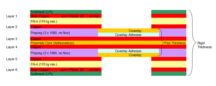 Figure
1: Example
of a standard 6-layer rigid-flex construction.
Figure
1: Example
of a standard 6-layer rigid-flex construction.
Rigid-Flex pcb Constructions with Odd Layer Counts
Figure 2 displays an example of an odd layer count construction. Most Engineers are familiar with rigid board design where even layer counts are a requirement. Although an odd layer count is a lesser known design, it is manufacturable and has its own set of benefits.
 Figure
2: Example
of an odd layer count rigid-flex construction.
Figure
2: Example
of an odd layer count rigid-flex construction.
Figure 2 shows a seven-layer rigid board with three flexible circuit layers. This odd layer construction is primarily used for designs that require two-sided shielding in the flex areas which is mostly driven by stripline impedance control. Some designs may have RF and EMI considerations. The ground / signal / ground construction is contained within the three layers of flex. It can also allow for a large number of interconnects between rigid sections.
The stack-up example illustrated in Figure 3 is more simplistic. This rigid-flex construction has been designed with five layers in the rigid area and only one layer of flex for part numbers that have a minimal number of rigid to rigid interconnects. It also provides a high degree of flexibility and reduces costs.