

2 - Ophir - тоже камеры
.pdfMODE-FIELD DIAMETER AND “SPOT SIZE” MEASUREMENTS OF LENSED AND TAPERED SPECIALTY FIBERS
By Jeffrey L. Guttman, Ph.D., Director of Technology, Ophir-Spiricon
ABSTRACT: The Mode-Field Diameter (MFD) and “spot size” of an assortment of lensed and tapered specialty fibers were determined from far-field and nearfield measurements.
In the far field, measurements were made using a 3D-scanning goniometric radiometer that provides a complete hemispherical profile. Indirect measures of the near field derived from these data are reported, including the Petermann II MFD, the 1/e2 spot size using the farfield Gaussian approximation, and a measure obtained from 2D Fourier transform inversion of the far field using phase retrieval techniques. In the near field, direct profile measurements were made using an IR Vidicon camera and magnifying objective lenses, with the spot size reported as the 1/e2 diameter of the imaged profile.
Lensed and Tapered specialty fibers are designed to optimize coupling between the fiber and various optical components such as edgeemitting laser diodes and AWGs. The light from these fibers forms a focus at some finite distance away from the fiber end. The MFD and corresponding spot size of these fibers is typically in the range of 5 microns or less. These small spot sizes and corresponding high divergence present challenges to near field and far field measurements. Typically the near-field measurements are limited by the optical performance, and the farfield measures must extend to very large angles. Results of measurements of 6 commercially available fibers are presented, including different type
lensed/tapered fibers (4 axially symmetric and 1 elliptical) and a standard single-mode fiber for reference. Also, since the focused beams are in free space, there are some fundamental questions as to the applicability of the MFD, a measure originally formulated to describe the field distribution within a fiber. Measurement Technique The fibers were coupled to a stable narrow-linewidth diode laser source operating at a nominal wavelength of 1550 nm and output power of approximately 7dBm. Far-field profiles were obtained using a 3D scanning goniometric radiometer, with optical dynamic range greater than 60 dB. This instrument provides NIST-traceable measures of MFD to the 0.5% level for single-mode fiber. The angular measurement range for each scan is ±90°, with sampling every 0.055°. By rotating the source about the scan plane, a full hemispherical measure of the far-field profile is obtained. The 3D profiles for each fiber in this study consist of 50 azimuthal scans at increments of 3.6° about the fiber axis. Near-field profile measurements were made using an IR Vidicon camera and 2 different magnifying objective lenses: a 100X NA 0.9 microscope objective intended for use in the visible and a 40X NA 0.48 aspheric lens designed for the IR. The point-spread function of this lens at 1550 nm is approximately 2.6 μm. The charac-
continued on page 22
B E A M P R O F I L I N G PagePage219
MODE-FIELD
DIAMETER
continued from page 21
teristics of the 100X lens at 1550nm are not known. |
ground level of the measurements, seen in figure 1a |
The fibers were positioned using a high precision |
for the profile of the standard single-mode fiber, is |
3-axis translation stage. Absorbing glass filters were |
at the -60dB level relative to the peak. The profiles of |
used for optical attenuation. The RS-170 camera |
the lensed/tapered fibers extend in all cases to ±90°. |
video images were acquired using a framegrabber |
The profiles for fibers #1-5 have the appearance of |
with 8-bit resolution, i.e., 256 levels. Measurement |
a superposition of a main beam and a scatter back- |
accuracy depends on the camera noise, sensor re- |
ground, probably due to surface modifications and |
sponse uniformity, the digitization, the number of |
defects introduced in the fabrication process. The |
pixels in the image, and on the optical properties |
angular extent of the main beam for these profiles |
of the lens used. With adequate pixel count and |
ranges from approximately ±30° for the standard sin- |
lens quality, the signal noise and sensor response |
gle-mode fiber to greater than ±70° for fiber #5. The |
provide accuracy to the ±3% level. Accuracy is also |
profile for fiber #6, the elliptical fiber, consists of a |
strongly dependent on the lens position because of |
main beam with a prominent diffraction structure. |
the short depth of focus of both the lens and the |
(Although not shown here, the scatter and diffrac- |
fibers being measured. Measurement Results Com- |
tion structure extend to angles greater than ±90°, in |
plete hemispherical far-field profiles of the 6 fibers, |
the backward direction.) |
(designated fibers # 1-6), and the corresponding 1D |
|
cross-sectional profiles through the principal axes of |
|
the distribution, are shown in figure 1. The back- |
|
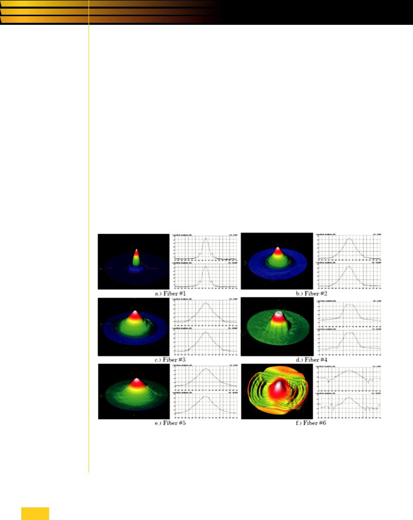
Figure 1. Complete hemispherical far field profiles of fibers # 1-6, and the corresponding 1D cross-sectional profiles through the principal axes of the distribution. The vertical scale is 10dB/division and the horizontal scale is 10°/division. Example images obtained in the near field for fiber #6, the elliptical fiber with the smallest spot size of all the fibers measured here, are shown in figure 2. The profile in figure 2a obtained with the 40X lens is clearly seen to be broadened by the spread function of the lens, and is also near the limit of adequate pixel count.
Page 22 O P H I R P H O T O N I C S , W W W . O P H I R O P T . C O M / P H O T O N I C S
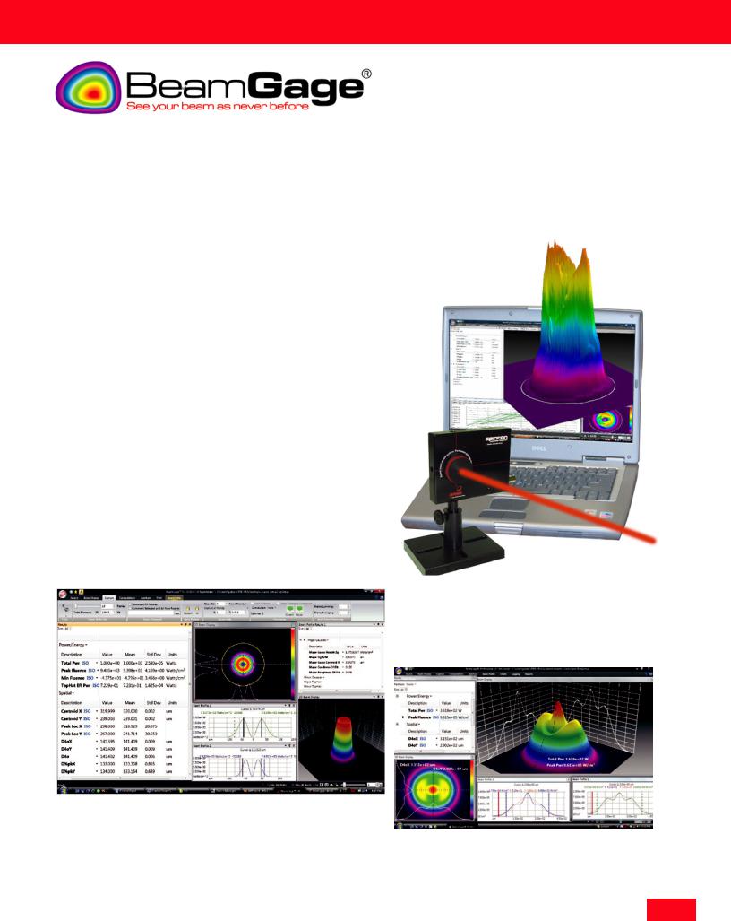
CAMERA-BASED PROFILING SYSTEMS
Take a laser beam and direcet some portion of the power onto the camera sensor array. Using BeamGage analysis software capture an image of the beam and make measurements of the spatial information in the beam. Camera-based beam profilers offers more details and true 3D analysis of the beam’s power density distribution when compared to scanning slit profilers. This allows complex mode patterns (like flat top and donut) to be identified while optimizing the laser systems.
•Different cameras to cover wavelengths from 13nm to 3000µm
•Beam diameters from 44µm to 20mm
•For CW and pulsed beams and single pulses
•Windowless sensor arrays
•Internal and external trigger for pulse synchronization
•Power/energy reading
•Optional NIST traceable power/energy reading
•55 separate measurement choices including all the ISO standards
•Statistical calculation on any measurement parameter
•Multiple charting options
•Beam pointing stability
•Pass/Fail flag on any measurement with external trigger signal on fail
•Image partitioning for analyzing multiple beams in the same image
•Automation interface with examples in LabVIEW, Excel and .Net VB
•Networking capability for accessing and sharing camera(s) over an
Ethernet LAN
BeamGage Main display Screen
Multiple Beam and Results Windows
B E A M P R O F I L I N G PagePage239
SLIT-BASED BEAM PROFILING SYSTEMS
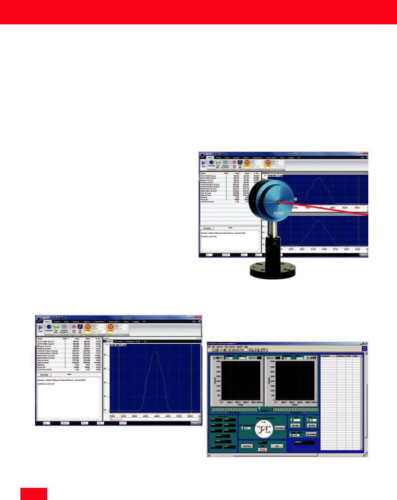
NanoScan
NanoScan uses moving slits, one of the ISO Standard scanning aperture techniques. Measurement is possible for beam sizes from microns to centimeters at beam powers from microwatts to kilowatts usually with little or no attenuation. Detector options—silicon, germanium, or pyroelectric—allow measurement at wavelengths from the ultraviolet to the far infrared. It can simultaneously measure multiple beams and offers an optional power meter for scanheads with silicon and germanium detectors.
•Wavelengths from UV to Far Infrared
Silicon detector—190-900nm Germanium detector—700-1800nm Pyroelectric detector—200nm to > 10.6µm
•Input beam diameter 8µm - 20mm; NanoScan type dependent
•Measures at beam powers from microwatts to over kilowatts with little or no attenuation
•Directly measure focus spot down to 7µm; NanoScan type dependent
•For CW and kHz pulsed beams
•Real time updates up to 20Hz
•7.5 orders of magnitude dynamic range allows real time adjustment of laser beams without need to adjust attenuation
•Optional power meter available with silicon and germa- nium detectors models
•Optional Automation interface
NanoScan Main Display Screen
Example of User Generated Automation
Interface Using Optional Pro Version
Page 24 O P H I R P H O T O N I C S , W W W . O P H I R O P T . C O M / P H O T O N I C S
ACCESSORIES FOR BEAM PROFILING
Spiricon has the most extensive array of accessories for beam profiling existing. There are components for attenuating, filtering, beam splitting, magnifying, reducing and wavelength conversion. There are components for wavelengths from the deep UV to CO2 wavelengths. Most of the components are modular so they can be mixed and matched with each other to solve almost any beam profiling requirement needed.
NEUTRAL DENSITY ATTENUATORS/FILTERS
Model |
Stackable |
LBF-50 |
Continuously |
ATP-K Variable Attenuator |
UV ND Filters |
|
ND Filters |
|
Variable |
|
|
|
ND1/ND2/ND3 |
|
|
|
|
Nominal ND value |
1,2,3 |
0.3, 0.7, 1, 2, 3, 4 |
1-6 continuously variable |
ND=1.7-4.6 |
0.3, 0.7, 1.0, 1.3, 1.7, 2.0, 2.3, |
|
|
|
|
Max. ND: 7.4 (with fixed |
2.7, 3.0, 3.3, 3.7, 4.0, 4.3, 4.7, |
|
|
|
|
)2.8 gray-glass attenuator |
5.0, 6.0 |
|
|
|
|
|
|
Clear aperature |
Ø19mm |
Ø12mm |
Ø20mm |
Ø15mm |
Ø20mm |
BEAM SPLITTER + NEUTRAL DENSITY
Model |
LBS-300 |
LBS-100 |
|
|
|
Wavelength |
multiple versions from 190 to 1550nm |
multiple versions; 400-900nm, 1064nm, 10.6µm |
Reflection |
0.01% of incident beam |
4% @ 400-900nm, 1% @1064nm, 0.5% or 5% @10.6µm |
|
|
|
Nominal ND value (vis) |
0.3, 0.7, 1, 2, 3, 4 |
0.3, 0.7, 1, 2, 3, 4 for 300-900nm & 1064nm 30% |
|
|
& 60% for 10.6µm |
Clear aperature |
Ø17.5mm |
Ø19mm |
BEAM SPLITTERS
Model |
Beam Tap l & ll |
|
Beam Tap l & ll YAG |
Stackable Beam Splitter |
Wavelength |
400-700nm |
|
1064nm |
190-2000nm |
Reflection |
4% & 0.16% of incident beam |
of incident beam 0.0025% & 0.5% |
5% & 0.025% of incident beam |
|
Clear aperature |
Ø17.5mm |
|
Ø17.5mm |
Ø15mm |
NEAR FIELD PROFILER |
BEAM REDUCERS AND EXPANDERS |
REIMAGING UV IMAGE |
||
FOR SMALL BEAMS |
|
|
CONVERTERS |
|
B E A M P R O F I L I N G PagePage259
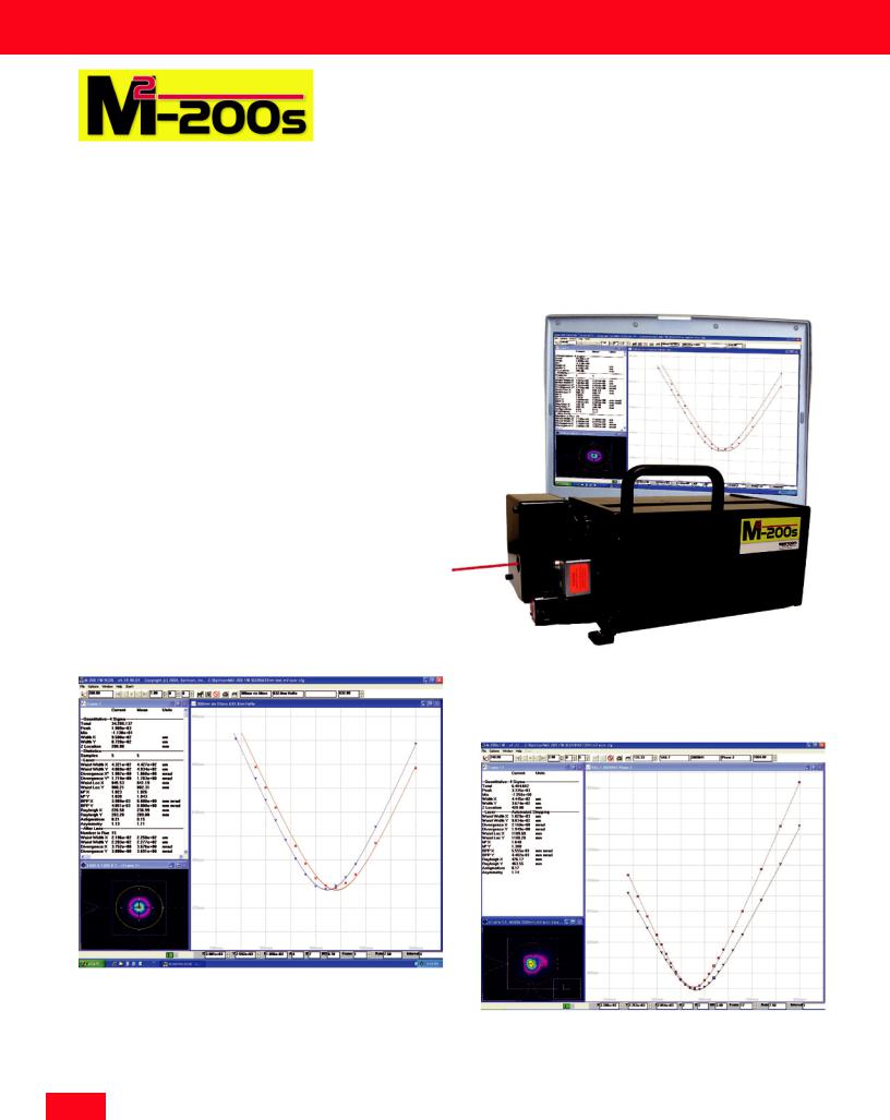
CAMERA-BASED BEAM PROPAGATION ANALYZER: M2
The M2-200s optical train uses a fixed position lens and camera. The mirrors that direct the focused beam into the camera are moved to precise locations, translating the beam through both the waist region and the far field regions. All these measurements and translations, as well as incremental beam attenuation, are automatically controlled by the M2-200s software. Spiricon’s M2-200s Beam Propagation Analyzer is fully ISO 11146 compliant.
•Wavelengths from 266 - 1300nm
•Input beam diameter 0.5 - 10mm
•Focus down to 44µm
•For CW and pulsed beams
•Windowless sensor arrays
•Automatically measure your beam quality in under 2 minutes
•Tune your laser for best operation
•ISO compliant
•Specifically developed for continuous usage
•Unequaled accuracy using patented UltracalTM Calibration
•Automatic attenuation adjustment
•Compact and portable
M2-200s Main Display Screen
M2-200s Display of a YAG Laser
Page 26 O P H I R P H O T O N I C S , W W W . O P H I R O P T . C O M / P H O T O N I C S

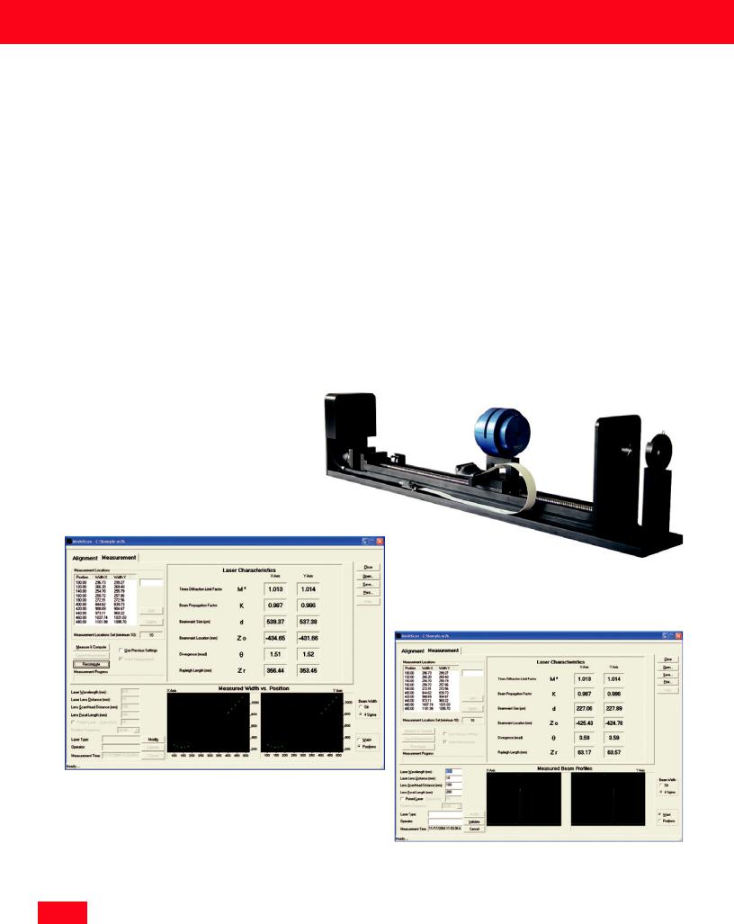
CAMERA-BASED BEAM PROPAGATION ANALYZER: M2
ModeScan 1780 – Real-Time Measurements
The ModeScan Model 1780 is a laser beam profiling instrument that measures the M² Beam Propagation Ratio and all associated ISO 11146 parameters instantaneously in real time at video rates to over 20Hz. The measurement technique, patented by Photon Inc., uses 10 reflective surfaces in the test space to form simultaneous replicas of the propagating beam at 10 locations on a CCD array camera. With all 10 measurement positions acquired at once, the instrument is suitable for measurement of both CW and pulsed lasers down to single-shot rates in the 1Hz or less range.
1780 Main Display Screen
1780 Measurement Display of 533 Laser
B E A M P R O F I L I N G PagePage279
SLIT-BASED BEAM PROPAGATION ANALYZER: M2
NanoModeScan 1740
For lasers with wavelengths in the UV and IR ranges which are either difficult or impossible to measure with a CCD based profiler, Photon has the Model 1740 NanoModeScan, which is also a dedicated, fully automated M² system using the NanoScan slit profiler to make the measurements according to the ISO 11146. NanoModeScan can make the entire M² measurement in as little as 20 seconds. The NanoModeScan is available with the Silicon, Germanium, or Pyroelectric NanoScan profiler, making it the only system that can measure M2 for lasers at any wavelength from <200nm to beyond 10.6µm.
•Wavelengths from UV to Far Infrared
Silicon detector—190-900nm Germanium detector—700-1800nm Pyroelectric detector—200nm to > 10.6µm
•Input beam diameter 10µm - 20mm; NanoScan type dependent
•Focus down to 7µm; NanoScan type dependent
•For CW and kHz pulsed beams
•Automated operation
•Measurement time usually less than 2 minutes
•Little or no attenuation needed for most lasers
•ISO compliant
1740 Measurement Display Screen
1740 Display of a 633nm Profile slice
Page 28 O P H I R P H O T O N I C S , W W W . O P H I R O P T . C O M / P H O T O N I C S
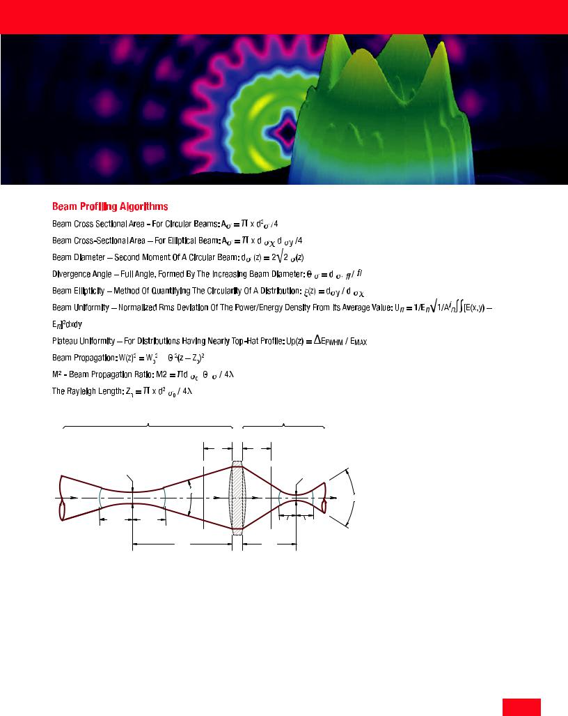
REFERENCE ALGORITHMS
"1 - space" |
lens |
"2 - space" |
|
f |
f |
|
|
W01 |
|
|
W02 |
|
|
|
|
|
|
|
Θ1 |
|
Z |
Θ2 |
|
|
|
||
ZR1 |
ZR1 |
ZR2 |
ZR2 |
|
|
|
|
||
|
Z01 |
Z02 |
|
|
H1 H2
ULTRACAL™ - Our patented, baseline correction algorithm helped establish the ISO 11146-3 standard for beam measurement accuracy. Ultracal ensures the highest accuracy and reliability in the industry by retaining negative signals essential for making correct beam width measurements and for extracting weak signals out of noise. Patent number: 5440338. UltraCal is part of our
.BeamGage laser beam analysis application
B E A M P R O F I L I N G PagePage299
REFERENCE ALGORITHMS
Page 30 O P H I R P H O T O N I C S , W W W . O P H I R O P T . C O M / P H O T O N I C S