

диафрагмированные волноводные фильтры / 6f951f5e-5988-44e7-af1c-cae65715aea8
.pdfRadio Science |
10.1002/2016RS006181 |
|
|
Figure 11. A 3-D model of the back to back transition simulated in CST. Separation between microstrip ports is 15 mm.
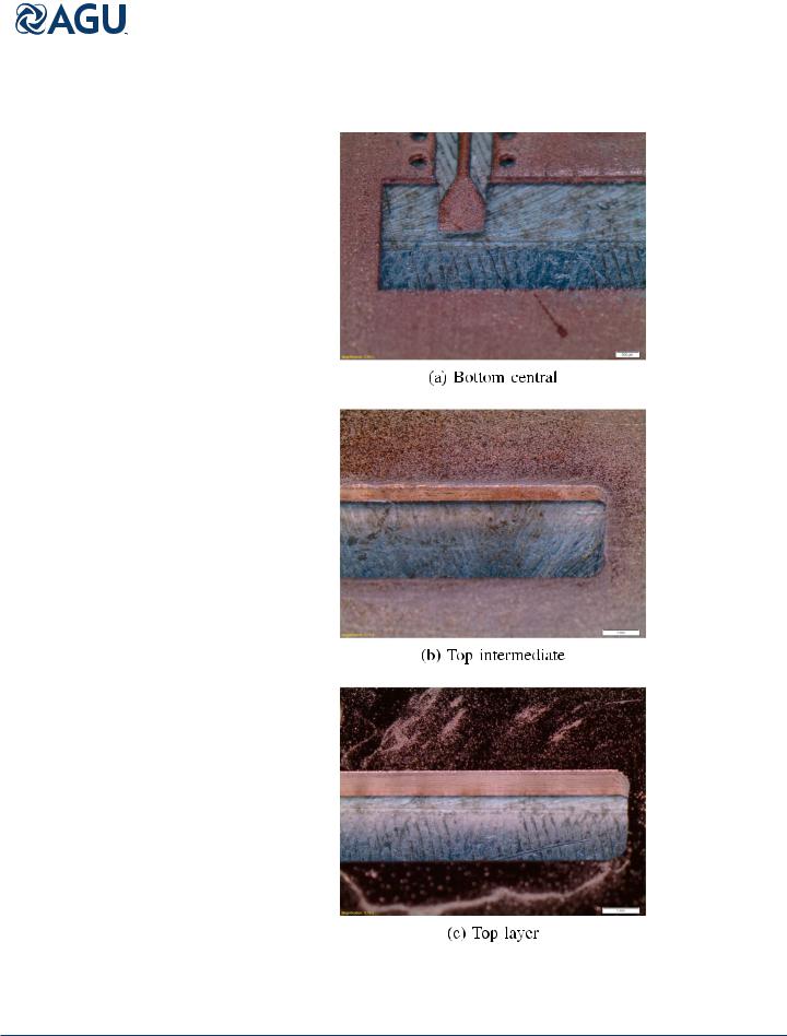
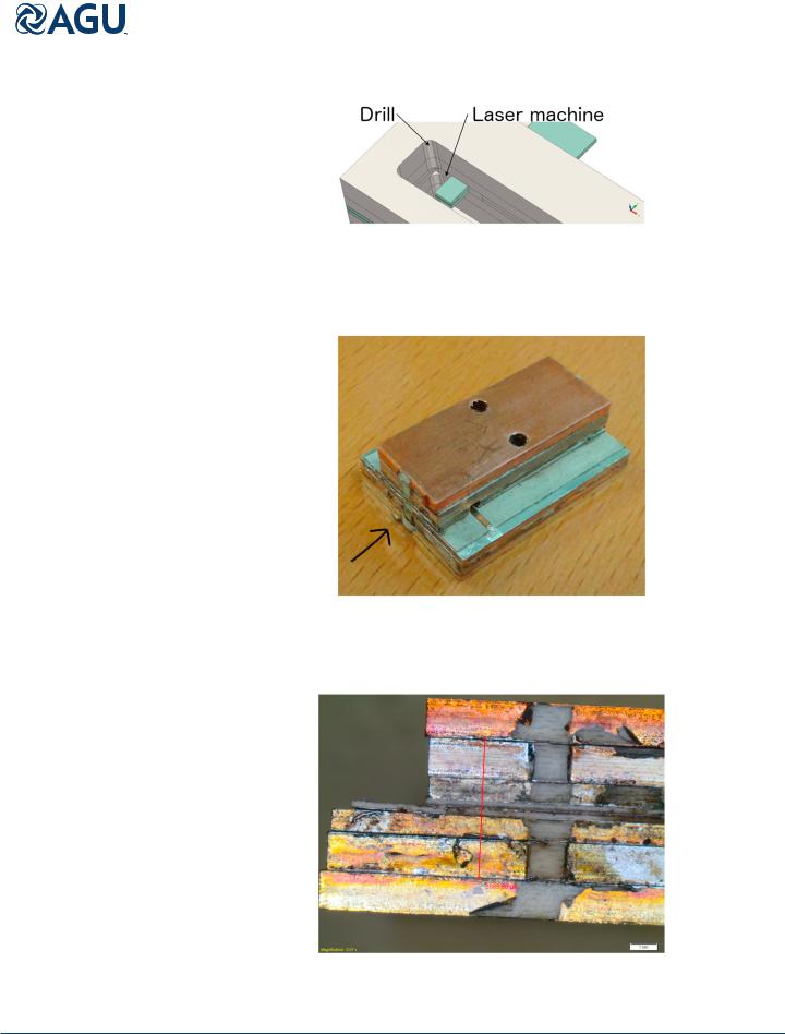
pins can be removed (see Figure 15). Figure 16 shows a lateral view of the assembled prototype, where all the PCB piled together can be observed in detail. The width of the synthesized waveguide (ESIW) has been measured, and the total width is 5.6 mm, very close to the ideal value.
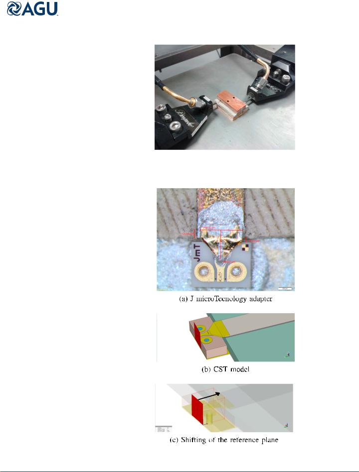
The measurement of the structure was performed in a small probe station equipped with coplanar probes of the company PicoProbe (see Figure 17). Commercial adapters from coplanar to microstrip lines of the J microTechnology company JMicroTechnology [2016] were used, with reference PP1003 (see Figure 18a). These adapters are connected to the microstrip lines of the prototype using golden strips with tapered shape. This method has proven to give better results than the use of bonding wires. The e ect of the adapters can be de-embeded from the measurements with the help of the calibration substrate provided by the company. However, the e ect of the golden tapered strips persists. Since this e ect cannot be de-embeded, the adapter and the tapered strips have been modeled with the CST full-wave commercial simulator and taken into account in the simulated results (see Figure 18b). The measured physical dimensions of the golden tapered strip shown in Figure 18a have been used for the CST model. Since the coplanar to microstrip adapters are de-embeded from the measurements, in the CST model the reference planes are shifted as shown in
Figure 12. Top view of one PCB with a thin bath of soldering paste.
BELENGUER ET AL. |
ESIW TECHNOLOGY FOR E PLANE DEVICES |
59 |
Radio Science |
10.1002/2016RS006181 |
|
|
Figure 13. Perspective view of di erent PCB of the manufactured prototype.
BELENGUER ET AL. |
ESIW TECHNOLOGY FOR E PLANE DEVICES |
60 |
Radio Science |
10.1002/2016RS006181 |
|
|
Figure 14. Perspective view of the CST model. Rounded corners have been considered for the drilled PCB, and square corners for the central PCB have been manufactured with a laser machine.
Figure 15. Perspective view of the manufactured back-to-back transition with all the PCB assembled.
Figure 16. Front view of the assembled back-to-back transition. Point of view is marked with an arrow in Figure 15. The measured width of the ESIW is 5.6 mm.
BELENGUER ET AL. |
ESIW TECHNOLOGY FOR E PLANE DEVICES |
61 |
Radio Science |
10.1002/2016RS006181 |
|
|
Figure 17. Measurement setup.
Figure 18. Coplanar to microstrip adapter PP1003 from J microTechnology.
BELENGUER ET AL. |
ESIW TECHNOLOGY FOR E PLANE DEVICES |
62 |
Radio Science |
10.1002/2016RS006181 |
|
|
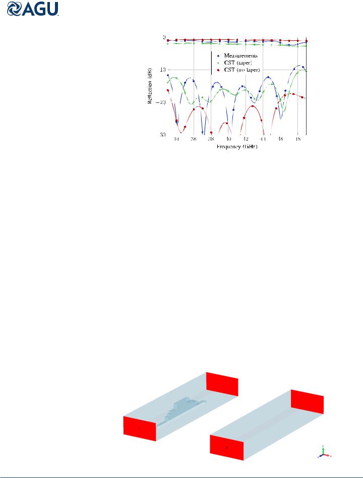
Figure 19. Simulation and measurements for the back-to-back transition of Figure 11.
Figure 18c, so that these adapters are also de-embeded from the simulation, and only the tapered strips are considered both in measurements and in simulation.
An Agilent Technologies network analyzer, model E8364A, was used for the measurements, which are compared with simulations in Figure 19. First, the commercial software CST has been used for simulating the whole structure without the golden tapered transitions of Figure 18. A conductivity of 107 S/m has been used to model the conducting surfaces, according to the predicted conductivity of an electrodeposited copper surface with roughness of 19 μm at the operating frequency [see Chen, 2007]. This gives an idea of the performance that can be achieved with the ESIW-E. It can be observed that these simulations predict return losses of over 20 dB and insertion losses lower than 1 dB in almost all of the recommended frequency band of operation for the WR22 (from 33 GHz to 49 GHz), which is the rectangular waveguide with the same width as the ESIW-E used for manufacturing this prototype. This proves the validity of the ESIW-E for the implementation of high-performance and high-frequency microwave circuits. This simulated results cannot be directly compared against measurements because the golden tapered transitions cannot be de-embeded from the measurements, as has already been discussed. Therefore, the measurements are compared in Figure 19 with the CST simulation including the golden tapered transition. It can be observed that there is a good agreement between simulation and measurements, which validates the design and the manufacturing process and proves that the performance is worsened as a consequence of the tapered transition. The measured insertion losses are slightly smaller than in simulation. This is probably due to the value of the conductivity that has been used, which was probably smaller than the real conductivity.
4. 90 ESIW-E Phase Shifter
E plane phase shifters for wide band applications and high frequency, such as radio astronomy, where sensitivity of the receiver increases with the bandwidth, are di cult to implement with H plane structures.
Figure 20. Schematic view of the CST model of the phase shifter and its reference line in a traditional WR-22 waveguide.
BELENGUER ET AL. |
ESIW TECHNOLOGY FOR E PLANE DEVICES |
63 |
Radio Science |
10.1002/2016RS006181 |
|
|
Figure 21. Dimensions of the designed phase shifter. The width of the ridge is w = 0.6 mm.
In Xu et al. [2005], Moldovan et al. [2006], and Cheng et al. [2007] SIW phase shifters are presented, but the bandwidth is not very large. The same occurs for the HSIW presented in Chen et al. [2007]. A broadband SIW phase shifter is presented in Cheng et al. [2010], but at the expense of presenting a physical length larger than that of the reference line. With the same physical length the phase shifter is narrow band. A broadband SIW phase shifter loaded with circular rods has been recently presented in Djerafi et al. [2015]. However, this solution would be di cult to implement for higher-frequency bands, where the required diameter of the rods would
Figure 22. CST simulation of the ridge phase shifter of Figure 20.
BELENGUER ET AL. |
ESIW TECHNOLOGY FOR E PLANE DEVICES |
64 |
Radio Science |
|
|
|
|
10.1002/2016RS006181 |
||
|
|
|
|||||
|
Table 3. Characteristics of All the PCB Used for the Manufacture of the |
||||||
|
Phase Shiftera |
|
|
|
|
|
|
|
Layer |
h |
t1 |
t2 |
ht |
PCB Name |
|
|
Top cover |
1.524 |
0.035 |
0.010 |
1.614 |
RO4003C |
|
|
Top layer |
1.524 |
0.035 |
0.010 |
1.614 |
RO4003C |
|
|
Top intermediate |
0.813 |
0.035 |
0.010 |
0.903 |
RO4003C |
|
|
Top central |
0.254 |
0.017 |
0.006 |
0.3 |
RO3003 |
|
|
Bottom central |
0.254 |
0.017 |
0.006 |
0.3 |
RO3003 |
|
|
Bottom intermediate |
0.813 |
0.035 |
0.010 |
0.903 |
RO4003C |
|
|
Bottom layer |
1.524 |
0.035 |
0.010 |
1.614 |
RO4003C |
|
|
Bottom cover |
1.524 |
0.035 |
0.010 |
1.614 |
RO4003C |
|
ah is the substrate height, t1 is the thickness of the substrate metallic layer, t2 is thickness of the electrodeposited metallic layer, and ht = h + 2t1 + 2t2 is the total height of the layer. All dimensions are in millimeter.
Figure 23. Schematic views of the ESIW-E phase shifter.
BELENGUER ET AL. |
ESIW TECHNOLOGY FOR E PLANE DEVICES |
65 |
Radio Science |
|
|
|
10.1002/2016RS006181 |
|
|
|
|
|
|
|
|
|
|
|
|
|
|
|
|
|
|
|
|
|
|
|
|
|
|
|
|
|
|
|
|
|
|
|
|
|
|
|
|
|
|
|
|
|
Figure 24. Measured reflections of the ESIW-E phase shifter and the reference line.
be too small. Besides, phase shifters in SIW or HSIW technology present high levels of insertion loss due to the presence of the dielectric. In ESIW-E, insertion losses will be smaller because the waves propagate through the air.
In order to test the performance of the ESIW-E for the implementation of high-frequency and highperformance microwave devices, a 90 phase shifter operating in the Q band (from 35 to 47 GHz) has been designed and manufactured.
The phase shifter provides a fixed phase shift, in this case 90 , with respect to a reference line. Therefore, two circuits must be manufactured, the phase shifter and the reference line.
The topology selected for the phase shifter is a traditional phase shifter in a ridge waveguide, where the waveguide is the ESIW-E and the ridge is manufactured using the two central PCB. Therefore, the width of the ridge is fixed by the height of these two central PCB (w = 0.6 mm).
Figure 20 shows the CST model of the phase shifter and its reference line implemented in a traditional WR-22 ridge waveguide.
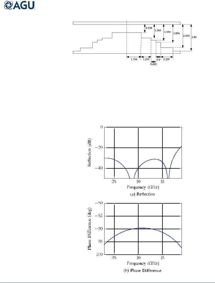
For the design of the phase shifter in WR-22 the classical deign procedure of Tribak et al. [2014] can be used, with the only limitation that the width of the ridge must be the width of the two central PCB (w = 0.6 mm with the choice of commercial substrates that we have used). As in Tribak et al. [2014], after finding an initial point with an equivalent monomode circuit, the full-wave multimode simulator Wave of Mician [2016] is used for optimizing, since it is highly e cient and allows a rapid optimization. The final dimensions of the designed phase shifter in WR-22 are shown in Figure 21.
BELENGUER ET AL. |
ESIW TECHNOLOGY FOR E PLANE DEVICES |
66 |
Radio Science |
|
|
|
10.1002/2016RS006181 |
|
|
|
|
|
|
|
|
|
|
|
|
|
|
|
|
|
|
|
|
|
|
|
|
|
Figure 25. Measured transmissions of the ESIW-E phase shifter and the reference line.
Figure 26. Measured amplitude and phase di erences of the ESIW-E phase shifter and the reference line.
BELENGUER ET AL. |
ESIW TECHNOLOGY FOR E PLANE DEVICES |
67 |

Radio Science |
10.1002/2016RS006181 |
|
|
Acknowledgments
This work was supported by the Ministerio de Economía y Competitividad, Spanish Goverment, under research projects TEC2013-47037-C5-3-R, TEC2013-47037-C5-1-R, AYA2013-49759-EXP, and CSD2010-00064. All the data related with this work can be
requested to H. Esteban writing to hesteban@dcom.upv.es
The simulated results of the CST model of Figure 20 are depicted in Figure 22. The return losses and the phase di erence with respect to the reference line are shown. It can be observed that the design provides, at simulation level, good matching (return loss over 30 dB) and quite stable phase di erence in the desired frequency band.
When the design in the classic rectangular waveguide is finished, it is mapped to an ESIW-E splitting the width
of the WR-22 into several PCB. Table 3 shows the characteristics of the PCB used for the manufacturing of the T3 phase shifter and its reference line. As it can be observed, the width of the ESIW-E with this choice of PCB is
a = 5.634 mm, which is slightly lower than the width of the standard WR-22 (a = 5.6896 mm). However, it is worth noting that the tin soldering paste used for assembling the PCB slightly increases the width of the ESIW-E.
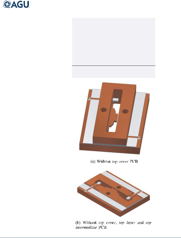
Figure 23 shows a schematic view of the ESIW-E phase shifter. It can be observed that the two central PCB form the ridge of the phase shifter. The reference line is similar but without the ridge steps.
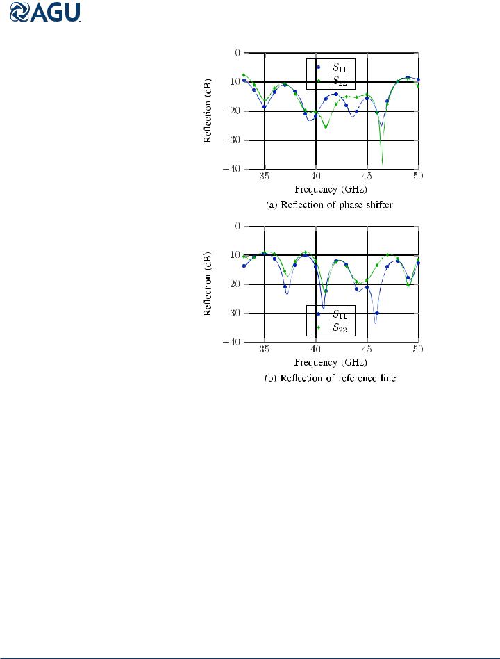
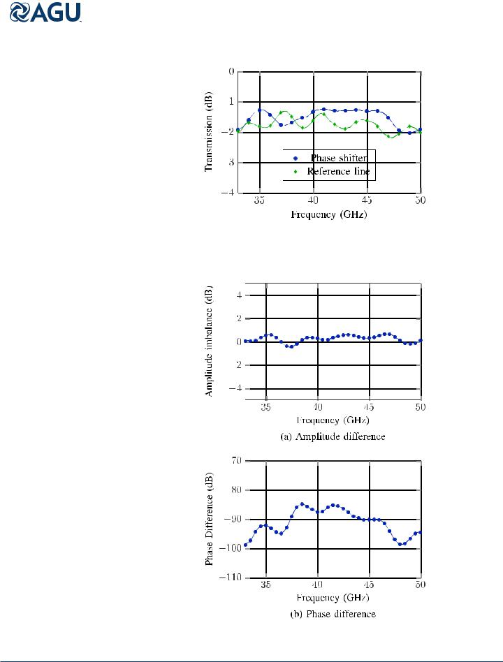
The phase shifter and the reference line were measured in the coplanar probe station of Figure 17, with the J microTechnology adapters from coplanar to microstrip line, plus the golden tapers. The measured reflections of the phase shifter and the reference line are depicted in Figure 24. The return losses for both the phase shifter and the reference line are greater than 10 dB in the frequency band of interest (from 35 to 47 GHz). If the e ect of the golden taper would be de-embeded from the measurements, the return losses would be higher. Figure 25 shows the transmission of both circuits. The insertion losses are lower than 2 dB. The amplitude and phase di erences are depicted in Figure 26. The mean phase di erence in the desired band is −89.1 with a maximum variation of ±5 . And the mean amplitude imbalance is 0.28 dB with a maximum variation of ±0.6 dB.
These results prove that the ESIW-E is a promising alternative for mapping E plane waveguide solutions in a low cost substrate integrated device. The E plane solutions cannot be mapped to SIW or ESIW. The performance is degraded when compared to the same device implemented in a classical rectangular waveguide, but the ESIW-E is low cost, integrated in a substrate and connected to planar microstrip ports, and its performance is much better than the performance of equivalent planar devices.
5. Conclusion
A new E plane empty substrate integrated waveguide (ESIW-E) has been presented. This new type of waveguide has the same advantages of other empty substrate integrated circuits (low cost, easy manufacturing, low losses compared to other SIC filled with substrate, higher-quality factor, and integration in a PCB), and it can easily map classical E plane solutions in rectangular waveguide, at the expense of needing more layers than the H plane ESIW.
A transition from microstrip to ESIW-E operating in a high-frequency band has been successfully designed, manufactured, and measured. A broadband high-frequency phase shifter has been implemented, and results prove the validity of this new type of circuit. The presence of a tapered transition from microstrip to coplanar waveguide (required for performing measurements at high frequencies with a probe station) increases the insertion losses and reduces the return losses, but it has been demonstrated with simulation that this e ect is caused by this transition that has not been de-embeded from the measurements.
References
Arregui, I., I. Arnedo, A. Lujambio, M. Chudzik, D. Benito, R. Jost, F. Görtz, T. Lopetegi, and M. Laso (2010), A compact design of high-power spurious-free low-pass waveguide filter, IEEE Microwave Wireless Compon. Lett., 20(11), 595–597, doi:10.1109/LMWC.2010.2072989.
Belenguer, A., H. Esteban, and V. Boria (2014), Novel empty substrate integrated waveguide for high-performance microwave integrated circuits, IEEE Trans. Microwave Theory Tech., 62(4), 832–839, doi:10.1109/TMTT.2014.2309637.
Bigelli, F., D. Mencarelli, M. Farina, G. Venanzoni, P. Scalmati, C. Renghini, and A. Morini (2016), Design and fabrication of a dielectricless substrate-integrated waveguide, IEEE Trans. Compon. Packag. Manuf. Technol., 6(2), 256–261, doi:10.1109/TCPMT.2015.2513077.
Budimir, D. (1997), Optimized E-plane bandpass filters with improved stopband performance, IEEE Trans. Microwave Theory Tech., 45(2), 212–220, doi:10.1109/22.557602.
Cassivi, Y., and K. Wu (2004), Substrate integrated nonradiative dielectric waveguide, IEEE Microwave Wireless Compon. Lett., 14(3), 89–91, doi:10.1109/LMWC.2004.824808.
Chen, J., W. Hong, P. Yan, B. Liu, Y. Wang, and K. Wu (2007), Design of a six-port junction using half-mode substrate integrated waveguide,paper presented at Asia–Pacific Microwave Conference 2007, APMC 2007, pp. 679–681, 11–14 Dec., doi:10.1109/APMC.2007.4554870.
Chen, J.-X., W. Hong, Z.-C. Hao, H. Li, and K. Wu (2006), Development of a low cost microwave mixer using a broad-band substrate integrated waveguide (SIW) coupler, IEEE Microwave Wireless Compon. Lett., 16(2), 84–86, doi:10.1109/LMWC.2005.863199.
BELENGUER ET AL. |
ESIW TECHNOLOGY FOR E PLANE DEVICES |
68 |